MIL- STD-883F 2004 TEST METHOD STANDARD MICROCIRCUITS.pdf - 第213页
MIL-STD-883F METHOD 2010.11 18 June 2004 3 f. Definitio ns: (1) Active circu it area . All areas enc losed by t he perimet er of f uncti onal ci rcui t element s, oper ating metal lizat ion or any connec ted combi nation…

MIL-STD-883F
METHOD 2010.11
18 June 2004
2
b. Sequence of inspection. The order in which criteria are presented is not a required order of examination and may
be varied at the discretion of the manufacturer.
When inverted die mounting techniques are employed, the inspection criteria contained herein that cannot be
performed after mounting shall be conducted prior to attachment of the die. Devices that fail any test criteria
herein are defective devices and shall be rejected and removed at the time of observation.
Visual criteria may be inspected as follows:
(1) Prior to die attachment without re-examination after die attachment; 3.1.1.2, 3.1.1.5, 3.1.1.7, 3.1.2, 3.1.4 e
and f, 3.1.5, 3.1.6 a-f, 3.2.6.
(2) Prior to bonding without re-examination after bonding; 3.2.3.
(3) For condition B only; the following criteria may be inspected prior to die attachment at high power, plus low
power after die attachment, provided a high magnification sample to sample size number = 45 accept
number C = 0 is performed at precap inspection; 3.1.1.1, 3.1.1.3, 3.1.1.4, 3.1.1.6, 3.1.3, 3.1.4 a-d and g-o,
3.1.6 g and h, 3.1.7. If the sample fails the entire lot shall be reinspected at high magnification for the failed
criteria.
c. Inspection control. In all cases, examination prior to final preseal inspection shall be performed under the same
quality program that is required at the final preseal inspection station. Care shall be exercised after inspections in
accordance with 3b, to insure that defects created during subsequent handling will be detected and rejected at
final preseal inspection. During the time interval between visual inspection and preparation for sealing, devices
shall be stored in a controlled environment. Devices examined to condition A shall be inspected and prepared for
sealing in a 100 (0.5 Hm or greater) particles/cubic foot controlled environment (class 5 of ISO 14644-1) and
devices examined to condition B criteria shall be inspected and prepared for sealing in a 100,000 (0.5 Hm or
greater) particles/cubic foot controlled environment (class 8 of ISO 14644-1), (see A.4.8.1.1.7 of appendix A of
MIL-PRF-38535), except that the maximum allowable relative humidity in either environment shall not exceed 65
percent. Devices shall be in covered containers when transferred from one controlled environment to another.
d. Magnification. "High magnification" inspection shall be performed perpendicular to the die surface with the device
under illumination perpendicular to the die surface. "Low magnification" inspection shall be performed with a
metallurgical or stereomicroscope with the device under suitable illumination. Low magnification may be
performed at an angle other than 90° to the die surface to facilitate the inspection. The inspection criteria of 3.2.1
may be examined at "high magnification" at the manufacturer's option.
e. Reinspection. When inspection for product acceptance is conducted subsequent to the manufacturer's
inspection, the additional inspection may be performed at any magnification specified by the applicable test
condition, unless a specific magnification is required by the acquisition document. When suspected defects or
deficiencies are noted, additional inspection may be performed at magnifications needed to evaluate or resolve
the suspect items.
*

MIL-STD-883F
METHOD 2010.11
18 June 2004
3
f. Definitions:
(1) Active circuit area
. All areas enclosed by the perimeter of functional circuit elements, operating metallization
or any connected combinations thereof excluding beam leads.
(2) Coupling (air) bridge
. A raised layer of metallization used for interconnection that is isolated from the
surface of the element.
(3) Block resistor
. A thin film resistor which for purposes of trimming is designed to be much wider than would
be dictated by power density requirements and shall be identified in the approved manufacturer's precap
visual implementation document.
(4) Contact Via
. The Via where dielectric material is etched away in order to expose the Under Bump
Metalization (UBM) on the bond pads or solder bump attach pads.
(5) Channel
. An area lying between the drain and the source of FET structures.
(6) Controlled environment
. Shall be 1,000 (0.5 Hm or greater) particles/cubic foot controlled environment
(class 6 of ISO 14644-1), (see A.4.8.1.1.7 of appendix A of MIL-PRF-38535), except that the maximum
allowable relative humidity shall not exceed 65 percent.
(7) Crazing
. The presence of numerous minute cracks in the referenced material, (e.g., glassivation crazing).
(8) Detritus
. Fragments of original or laser modified resistor material remaining in the kerf.
(9) Die Coat
. A thin layer of soft polyimide coating applied to the surface of a semiconductor element that is
intended to produce stress relief resulting from encapsulation and to protect the circuit from surface scratches.
(10) Dielectric isolation
. Electrical isolation of one or more elements of a monolithic semiconductor integrated
circuit by surrounding the elements with an isolating barrier such as semiconductor oxide.
(11) Dielectric layer or layers
. Dielectric layer or layers deposited on the die surface to protect the redistribution
metalization, and to create the contact via for solder bump pad.
(12) Diffusion tub
. A volume (or region) formed in a semiconductor material by a diffusion process (n- or p- type)
and isolated from the surrounding semiconductor material by a n-p or p-n junction or by a dielectric material
(dielectric isolation, coplanar process, SOS, SOI).
(13) Foreign material
. Any material that is foreign to the microcircuit or package, or any nonforeign material that
is displaced from its original or intended position within the microcircuit package.
(14) Functional circuit elements
. Diodes, transistors, crossunders, capacitors, and resistors.
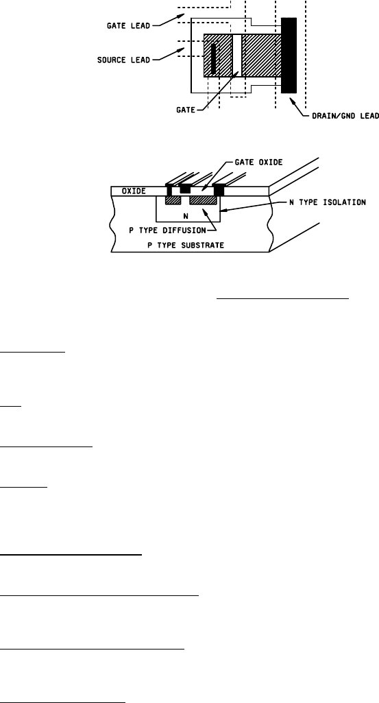
(15) Gate oxide
. The oxide or other dielectric that separates gate metallization (or other material used for the
gate electrode) from the channel of MOS structures (see figure 2010-1).
(16) Glassivation
. The top layer(s) of transparent insulating material that covers the active circuit area, with the
exception of bonding pad areas and beam leads.
(17) Glassivation cracks
. Fissures in the glassivation layer.
*
MIL-STD-883F
METHOD 2010.11
18 June 2004
4
FIGURE 2010-1. P channel MOS transistor
.
(18) Junction line
. The outer edge of a passivation step that delineates the boundary between "P" and "N" type
semiconductor material. An active junction is any P/N junction intended to conduct current during normal
operation of the circuit element, (e.g., collector to base).
(19) Kerf
. That portion of the component area from which material has been removed or modified by trimming or
cutting.
(20) Line of separation
. Visible distance or space between two features that are observed not to touch at the
magnification in use.
(21) MESFET
. (Metal semiconductor field-effect transistor). A field-effect transistor in which a metal
semiconductor rectifying contact is used for the gate electrode. Typically the structure is fabricated in
gallium arsenide and the term GaAs MESFET may be used. Both depletion-type and enhancement type
devices have been manufactured. The acronyms are D-MESFET, and E-MESFET, respectively.
(22) Metallization nonadherence
. Unintentional separation of material from an underlying substrate excluding air
bridges and undercutting by design.
(23) Multilayered metallization (conductors)
. Two or more layers of metal or any other material used for
interconnections that are not isolated from each other by insulating material. The term "underlying metal"
shall refer to any layer below the top layer of metal (see figure 2010-2).
(24) Multilevel metallization (conductors)
. Two or more levels of metal or any other material used for
interconnections that are isolated from each other by insulating material (also referred to as interlevel
dielectric) (see figure 2010-3).
(25) Narrowest resistor width
. The narrowest portion of a given resistor prior to trimming.