MIL- STD-883F 2004 TEST METHOD STANDARD MICROCIRCUITS.pdf - 第419页
MIL-STD-883F METHOD 2032.2 18 June 2004 13 Cla ss H Class K 3.1.1 .8 Metalliz ed thr ough-hole defect s, "high magni fic ation" . No element shall be ac cept able that exhibi ts: a. Thr ough-hole metal lizat io…
MIL-STD-883F
METHOD 2032.2
18 June 2004
12
Class H Class K
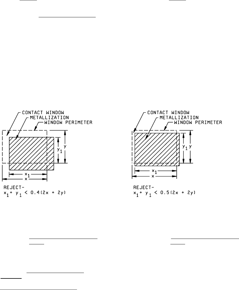
3.1.1.6 b. A contact window that has less than a 3.1.1.6 b. 50 percent of its perimeter
continuous 40 percent of its perimeter
(see figure 2032-7k).
covered by metallization (see figure
2032-7h).
NOTE: When, by design, metallization
is completely contained in a contact
window, or does not cover the entire
contact perimeter, 3.1.1.6a, area
coverage, or 3.1.1.6b, perimeter
coverage, can be deleted as applicable
provided that the design criteria are
satisfied.
FIGURE 2032-7h. Class H metallization alignment
FIGURE 2032-7k. Class K metallization alignment
criteria
. criteria.
c. A metallization path not intended to cover c. Same as Class H.
a contact window that is separated from
the window by less than 0.1 mil unless
by design
.
3.1.1.7 Metallization bumps or indentations
.
a. For capacitors only, a bump or indentation a. Same as class H.
in the overlaying metallization.
MIL-STD-883F
METHOD 2032.2
18 June 2004
13
Class H Class K
3.1.1.8 Metallized through-hole defects,
"high magnification"
. No element shall be
acceptable that exhibits:
a. Through-hole metallization that is not a. Same as class H.
vertically continuous or that does not
cover at least a continuous 50 percent
of the inside, circumferential surface
area unless by design.
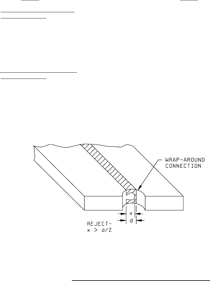
3.1.1.9 Wrap-around connection defects,
"high magnification"
. No element shall be
acceptable that exhibits:
a. Unmetallized area in the edges of a. Same as class H.
wrap-around connections greater than 50
percent of the largest dimension of the edge
metallization (see figure 2032-8h).
FIGURE 2032-8h. Class H wrap-around connection unmetallized area criterion
.
MIL-STD-883F
METHOD 2032.2
18 June 2004
14
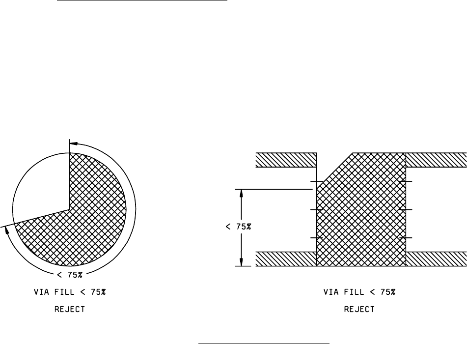
3.1.1.10 Substrate plug via defects, “low magnification”. When inspected from each side of the substrate, no element
shall be acceptable that exhibits:
a. A complete void through the via.
b. Any lifting, peeling, or blistering of the via metallization.
c. Via fill less than 75% of the total surface area of the via plug and less than 75% of the substrate thickness.
NOTE: These are minimum requirements. Via flatness and other requirements shall be in accordance with the
applicable detail drawings. The via fill may consist of thick film metallization.
FIGURE 2032-8Bh. Classes H and K via plug fill criteria