MIL- STD-883F 2004 TEST METHOD STANDARD MICROCIRCUITS.pdf - 第259页
MIL-STD-883F METHOD 2010.11 18 June 2004 49 Condition A Conditi on B Class le vel S Class lev el B 3.2.5 For eign materi al . Die i nspect ions s hall be at high magnifi cati on. Pack age and lid i nspect ions s hall be …
MIL-STD-883F
METHOD 2010.11
18 June 2004
48
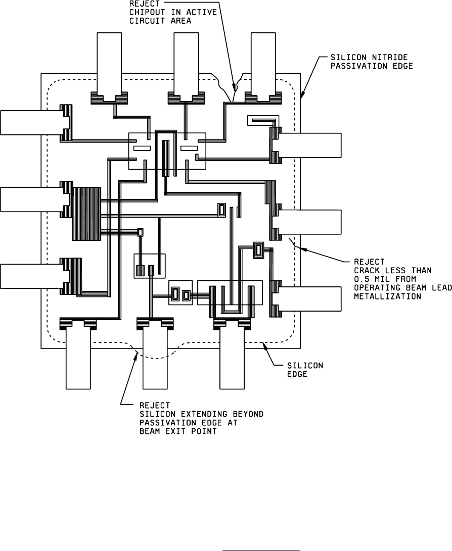
FIGURE 2010-38. Beam lead die faults
.

MIL-STD-883F
METHOD 2010.11
18 June 2004
49
Condition A Condition B
Class level S Class level B
3.2.5 Foreign material
. Die inspections shall be at high magnification. Package and lid inspections shall be at low
magnification. Die criteria may be examined at high magnification prior to die mounting provided they are re-examined at
low magnification during preseal inspection. No device shall be acceptable that exhibits:
NOTE: Foreign material may be removed, if possible, by subjecting the device to a nominal gas blow (less than 25 psig).
After this gas blow off at inspection, all wire bonded devices shall be inspected/reinspected for possible wire damage.
Use of a higher psig value is permitted provided that the manufacturer has characterized the process and has data to
assure that no damage is done to the wire bonds. This data shall be available upon request to the preparing or
acquiring activities.
a. Foreign particle(s) on the surface of the die that is (are) large enough to bridge the narrowest spacing between
unglassivated operating material (e.g., metallization, bare semiconductor material, mounting material, bonding
wire, etc.).
b. Foreign particle(s) other than on the surface of the die within the package or on the lid or cap that is (are) large
enough to bridge the narrowest spacing between unglassivated operating materials and are not the following:
Semiconductor material, glass splatter, gold imperfections in the die attach area, gold eutectic material or
package ceramic material.
NOTE: As an alternative to 100 percent visual inspection of lids or caps, the lids or caps may be subjected to a
suitable cleaning process and quality verification, approved by the qualifying activity. The lids or caps shall
subsequently be held in a controlled environment until capping or preparation for seal.
c. Foreign material attached to or embedded in the die surface that appears to bridge the active circuit elements
including metallization unless verified as only attached but not embedded by high power dark field illumination.
d. Liquid droplets, chemical stains, ink, or photoresist on the die surface that appear to bridge any combination of
unglassivated metallization or bare semiconductor material areas.
e. A particle of gold eutectic material, package ceramic material or semiconductor material, not attached to the die,
large enough to bridge the narrowest spacing between unglassivated operating materials, that does not exhibit a
minimum of 50 percent cumulative peripheral fillet or whose height is greater than the longest base dimension.
NOTE 1: This criteria shall not be cause for rejection
when the assembly process contains a gas blow (less
than 60 psig) after die attach and again Less than 25
psig) after wire bond provided rejectable materials (not
attached and large enough to bridge) have been removed
from the cavity.
NOTE 2: Gold imperfections in the die attach area that do not interfere with proper die attachment, sealing glass splatter
(provided it does not suggest inadequately controlled process and does not interfere with the die attach area) or
internal glass run out from frit seal (provided it is confined to package walls and does not interfere with the die
attach area) are not rejectable.

MIL-STD-883F
METHOD 2010.11
18 June 2004
50
Condition A Condition B
Class level S Class level B
3.2.5.1 Foreign material, die coated devices
. This inspection and criteria shall be required on all devices that receive a
die coat during the assembly process. This inspection will be done after die coat cure. No device shall be acceptable that
exhibits:
a. Unattached foreign particles on the surface of the die coat or within the package that is (are) large enough to
bridge the narrowest spacing between unglassivated operating material (e.g., metallization, bare semiconductor
material, mounting material, bonding wire, etc.). Note: Semiconductor particles shall be considered as foreign
material.
b. Partially embedded foreign material with an "unembedded portion" that is large enough to bridge the narrowest
spacing between unglassivated operating material (e.g., metallization, bare semiconductor material, mounting
material, bonding wire, etc.).
c. Foreign material attached to or embedded in the die coat that appears to bridge unglassivated operating material
when viewed from above (e.g., bare semiconductor material, bond pads, bonding wire, mounting material, etc.).
d. Embedded foreign particles that penetrate the entire thickness of the die coating.
3.2.5.1.1 Die coating material
. No device shall be accepted that exhibits:
a. Surface scratches that penetrate the die coating and expose underlying glassivated metal.
b. Die coating that is lifted or is peeling from the semiconductor surface.
3.2.6 GaAs backside metallization
. GaAs inspection shall be performed with low magnification prior to die mounting.
(Verification at high magnification is permitted.) With the approval of the acquiring activity, the manufacturer may substitute
a sample inspection plan at the wafer level for 100 percent inspection in dice form. The sample inspection plan shall be
documented in the manufacturer's baseline documentation and shall be performed to the requirements of test method 5013.
No devices shall be acceptable that exhibit the following.
a. Evidence of metal corrosion, lifting, peeling, blistering.
b. Voids or scratches that expose underlying metal or substrate whose cumulative areas are more than 25 percent of
the cell area or device area.
NOTE: Absence of gold in the die separation area (saw street) of devices with electroplated backside metallization is
not a cause for rejection. Small voids at edges due to die separation are acceptable if they comprise less
than 10 percent of the backside area.
c. Any voids or scratches in the substrate via metallization that effects more than 25 percent of the metallization or
cause unintended isolation of the metallization path.
d. Underetched vias.
e. Overetched vias.
4. SUMMARY
. The following details shall be specified in the applicable acquisition document.
a. Test condition (see 3).
b. Where applicable, any conflicts with approved circuit design topology or construction.
c. Where applicable, gauges, drawings, and photographs that are to be used as standards for operator comparison
(see 2).
d. Where applicable, specific magnification (see 3).