MIL- STD-883F 2004 TEST METHOD STANDARD MICROCIRCUITS.pdf - 第638页
MIL-STD-883F METHOD 5007.6 19 August 1994 2 TABL E I. W afer lo t accepta nce tests . Test Condit ions 1 / Limits 3 / Sampli ng plan 1. Wafer thickne ss Measurement shall be perfor med after final l ap or poli sh. Al l r…

MIL-STD-883F
METHOD 5007.6
19 August 1994
1
METHOD 5007.6
WAFER LOT ACCEPTANCE
1. PURPOSE
. This method establishes the requirements for the lot acceptance testing of microcircuit wafers intended for
class level S use.
2. APPARATUS
. The apparatus used shall be in accordance with the apparatus requirements of the methods specified
in the conditions column of table I.
3. PROCEDURE
. The performance of the wafer lot acceptance tests shall be in accordance with the conditions specified
in table I. If a lot fails a test under the sampling plan, as an alternative to rejecting the entire lot, the manufacturer may elect
to test each wafer in the lot for that parameter(s). All wafers successfully passing the test(s) shall be considered the lot for
the remainder of the tests. All wafers failing any test shall be removed from the lot. Data obtained from all tests shall be
recorded. The sequence of the tests in table I does not have to be adhered to, however, the tests must be performed at the
point in the processing (if specified) required in the conditions column of table I. Where limits are based on tolerances about
an "approved design nominal", the nominal shall be stated in the maintenance plan submitted for approval to the qualifying
or acquiring activity. Where table I limits are based on tolerances about the "mean", the mean shall be determined initially
on measurements from a minimum of five lots and the mean shall be stated in the maintenance plan submitted for approval
to the qualifying or acquiring activity. In no case shall the "design nominal" or "mean" exceed the absolute limits specified in
table I.
4. SUMMARY
. The following detail shall be specified in the applicable device specification:
Requirements or limits if other than those on table I.
MIL-STD-883F
METHOD 5007.6
19 August 1994
2
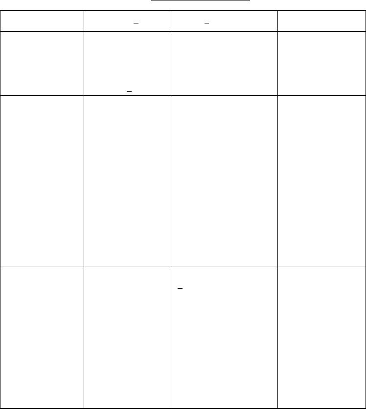
TABLE I. Wafer lot acceptance tests.
Test
Conditions 1/ Limits 3/ Sampling plan
1. Wafer thickness Measurement
shall be performed
after final lap
or polish. All
readings shall be
recorded. 2
/
Maximum deviation of
±2 mil from approved
design nominal 6 mil
minimum.
Two wafers per
lot. Reject lot
if any measurement
exceeds limits or
revert to test of
each wafer.
2. Metallization
thickness
All readings
shall be
recorded.
a. Conductor: 8 kÅ
minimum for single
level metal and for
the top level of
multi-level metal;
5 kÅ minimum for lower
levels, with a maximum
deviation of ±20
percent from the
approved design
nominal.
b. Barrier: Maximum
deviation of ±30
percent from the
approved design
nominal.
One wafer (or
monitor) per lot.
Reject lot if
measurement ex-
ceeds limits or
revert to test
of each wafer.
3. Thermal sta-
bility (ap-
plicable to:
All linear;
all MOS; all
bipolar digi-
tal operating
at 10 V or
more)
Record V
FB
or V
T
.
a. ∆V
FB
or ∆V
T
<
0.75, normalized to
an oxide thickness of
1000Å for bipolar
digital devices oper-
ating at 10 volts or
greater and all
bipolar linear devices
not containing MOS
transistor(s). The
monitor shall have an
oxide and shall be
metallized with the
lot.
One wafer (or
monitor) per lot.
Reject lot if
measurement ex-
ceeds limits or
revert to test
of each wafer.
See footnotes at end of table.
MIL-STD-883F
METHOD 5007.6
19 August 1994
3
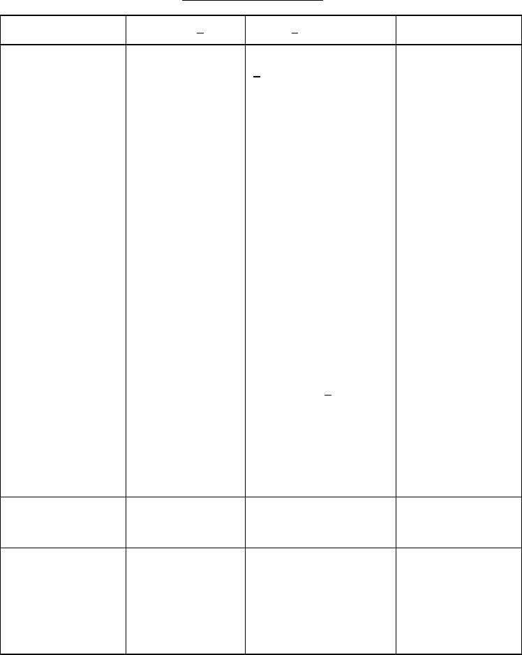
TABLE I. Wafer lot acceptance tests - Continued.
Test
Conditions 1/ Limits 3/ Sampling plan
3. Thermal sta-
bility (ap-
plicable to:
All linear;
all MOS; all
bipolar digi-
tal operating
at 10 V or
more)
Record VFB
or V
T
.
b. ∆V
FB
or ∆
VT
<
1.0 V,normalized to
an oxide thickness of
1,000Å for bipolar
linear devices that
operate above 5 V and
containing MOS tran-
sistor(s), and digital
devices that operate
above 10 V and
containing MOS
structures.
The V
FB
limit shall
not be exceeded by the
sum of the absolute
values of the MOS
oxide transistors and
the metallization ∆.
The monitor(s) shall
be oxidized and
metallized with the
lot. Separate
monitors may be used
for this test.
c. ∆V
FB
or V
T
<0.4 V,
normalized to an oxide
thickness of 1,000Å
for MOS devices. A
monitor consisting of
a gate oxide
metallized with the
lot shall be used.
One wafer (or
monitor) per lot.
Reject lot if
measurement ex-
ceeds limits or
revert to test
of each wafer.
4. SEM MIL-STD-883,
method 2018.
MIL-STD-883,
method 2018.
MIL-STD-883,
method 2018. Lot
acceptance basis.
5. Glassivation
thickness
All readings
shall be
recorded.
6 kÅ minimum for
Si0
2
and 2 kÅ
for Si
3
N
4
with
maximum deviation of
±20 percent from
approved design
nominal.
One wafer (or
monitor) per lot.
Reject lot if any
measurement ex-
ceeds limits
or revert to test
of each wafer.
See footnotes at end of table.