MIL- STD-883F 2004 TEST METHOD STANDARD MICROCIRCUITS.pdf - 第679页
MIL-STD-883F METHOD 5010.4 18 June 2004 29 APPENDIX II 40.3 PM eval uation . PM st ructures shall be submit ted for appr oval. W afer acc eptance wi ll be made on a waf er by wafer basis depending up on the inf orm ation…
MIL-STD-883F
METHOD 5010.4
18 June 2004
28
APPENDIX II
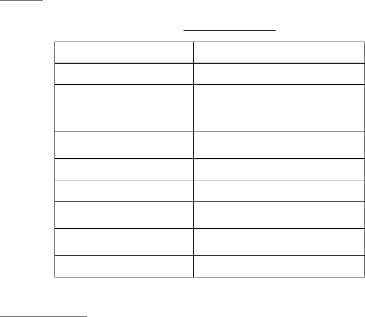
40.1 Processing
. Table II presents a minimum checkpoint list for wafer processing. If certain parameter values are
proprietary, they may be presented in normalized or other specialized form.
TABLE II. In-process check points
.
Process step
Inspection
Incoming material inspection Water, wafers, chemicals, gasses
Photolithography Spin speed, thickness, critical
dimension measurements, alignment,
post development visual inspection
(100X)
Oxidation Index of refraction, flatband, and
threshold voltage shifts, thicknesses
Diffusion Resistivity
Ion implant Resistivity, range, species
Deposition Thickness, resistivity, index of
refraction
Etching Critical dimension measurements,
etch rates, end point detection
SEM Step coverage (all metallization layers)
40.2 Visual/SEM inspection
. Visual inspection of photo resist (PR) patterns, alignment verniers, and critical dimension
measurements shall be made after each PR develop/bake operation. Following every etch and every ion implant, PR mask
stripped wafers shall be inspected for proper PR removal, damage, or other defects, and defective wafers removed from the
lot for scrap or for rework.
In-line nondestructive SEM inspection in accordance with MIL-STD-883, method 2018, shall be performed on each wafer lot.
One wafer from each metallization level shall be randomly selected for inspection. SEM inspection for each level may be
reduced to a weekly basis for each fabrication process when five consecutive lots pass inspection for the given level. If a
metallization level fails the weekly inspection, then lot by lot inspection shall be required until five consecutive lots again
pass. Wafers failing to meet the requirements of the test method shall be removed from processing. Wafer lot acceptance
shall be in accordance with table IV herein.
MIL-STD-883F
METHOD 5010.4
18 June 2004
29
APPENDIX II
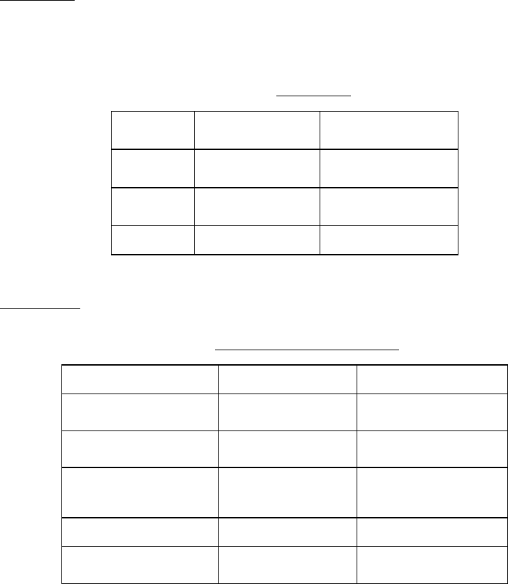
40.3 PM evaluation
. PM structures shall be submitted for approval. Wafer acceptance will be made on a wafer by wafer
basis depending upon the information derived from PM room temperature testing in accordance with table III. If drop-in
PM's are utilized, each wafer shall have at least 5 PM's; one shall be stepped in the center and the others in each of the
quadrants. For kerf PM's and PM's on individual die, the five probed PM's shall be located in the center and in each of the
quadrants. Quadrant PM's shall lie at least two-thirds of a radius away from the wafer center. Wafer acceptance will be
governed by table III.
TABLE III. PM evaluation
.
PM type
Number within PM
specification limits
Less than 3 out of 5
Drop-in
Reject
Kerf
Reject
Each die
Reject
40.4 Lot acceptance
. Acceptance requirements are as defined in table IV.
TABLE IV. Wafer lot acceptance requirements
.
Requirement
Condition Acceptance
Line certified MIL-PRF-38535
Appendix A
Control to specification
Lot traveler check points MIL-PRF-38535
Appendix A
100 percent in specifi-
cation for lot acceptance
PM test data Every wafer 75 percent of wafers in
lot pass PM evaluation,
otherwise reject.
Visual inspection Every wafer Wafer by wafer
SEM inspection MIL-STD-883
Method 2018
Method 2018 criteria

MIL-STD-883F
METHOD 5010.4
18 June 2004
30
APPENDIX II
40.5 Test results
. When required by the applicable document, the following test results shall be made available for each
lot submitted for qualification or quality conformance.
a. Results of each test conducted; initial and any resubmission.
b. Number of wafers rejected.
c. Failure analysis data and failure mode of each rejected SEC and the associated mechanism for catastrophic
failures for each rejected device.
d. Number of reworked wafers and reason for rework.
e. Read and record data of PM electric parameter measurements.
40.6 Defective devices
. All wafers that fail any test criteria shall be removed at the time of observation or immediately at
the conclusion of the test in which the failure was observed. Once rejected and verified as a failure, no wafer may be
retested for acceptance.