MIL- STD-883F 2004 TEST METHOD STANDARD MICROCIRCUITS.pdf - 第521页
MIL-STD-883F METHOD 3016 29 November 1985 1 METHOD 3016 ACTI VATION TIME VERIFI CATION 1. PURPOSE . This method est ablis hes a means f or ass uring c irc uit per form ance duri ng cold temper ature s tart up. It defines…
MIL-STD-883F
METHOD 3015.7
22 March 1989
6
NOTES:
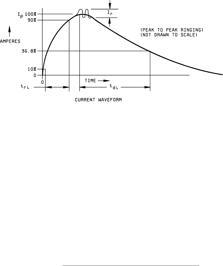
1. The current waveforms shown shall be measured as described in the waveform verification procedure of 3.2,
using equipment meeting the requirements of 2.
2. The current pulse shall have the following characteristics:
Tri (rise time) ---------------Less than 10 nanoseconds.
Tdi (delay time) ------------150 ±20 nanoseconds.
I
p
(peak current) -----------Within ±10 percent of the I
p
value shown in table II for the voltage step selected.
I
r
(ringing) -------------------The decay shall be smooth, with ringing, break points, double time constants or
discontinuities less than 15 percent I
p
maximum, but not observable 100
nanoseconds after start of the pulse.
FIGURE 3015-2. EDS classification test circuit waveforms (human body model)
.
MIL-STD-883F
METHOD 3016
29 November 1985
1
METHOD 3016
ACTIVATION TIME VERIFICATION
1. PURPOSE
. This method establishes a means for assuring circuit performance during cold temperature start up. It
defines an activation time for digital microelectronic devices such as TTL, DTL, RTL, ECL, and MOS and establishes the
procedure necessary to accomplish the required testing. This method will ensure that a specified capability is available a
known time interval after application of power.
1.1 Definitions
. The following definitions shall apply for the purposes of this test method:
a. Activation time. Activation time is defined as the time required for a device to become functionally operable after
initial power is applied at the operating temperature extremes as specified by the applicable acquisition document.
Note that activation time may be due to device and test system limitations, or both.
b. Maximum and minimum. Maximum and minimum refer to an algebraic system where "max" represents the most
positive value of the range and "min" represents the least positive value of the range. This is consistent with
MIL-STD-1331, 30.1 and 30.2 for logic levels only.
c. Maximum operating frequency. Maximum operating frequency is defined as the frequency of operation resulting
from use of the minimum clock period for devices requiring a clock, or the frequency of operation resulting from the
use of the minimum cycle time for devices not requiring a clock (such as memory devices) as specified in the
applicable acquisition document.
1.2 Symbols
. The following symbols and definitions shall apply for the purposes of this method.
1.2.1 Logic levels
.
a. V
LW
= worst case nominal low level logic input. The maximum allowable V
IL
specified in the applicable acquisition
document minus 100 millivolts to allow for uncertainty in the drive level capability of high speed functional test
equipment. (V
LW
= V
IL
(max) - 100 mV).
b. V
HW
= worst case nominal high level logic input. The minimum allowable V
IH
as specified by the applicable
acquisition document plus 100 millivolts (V
HW
= V
IH
(min) + 100 mV).
c. V
OH
(min) = minimum output high level specified for a digital microelectronic device.
d. V
OL
(max) = maximum output low level specified for a digital microelectronic device.
1.2.2 Activation times
.
a. t
AH
= maximum allowable activation time requirement, measured at V
CC
(max).
b. t
AL
= maximum allowable activation time requirement, measured at V
CC
(min).
2. APPARATUS
. An instrument shall be provided which has the capability of applying sequential logic patterns to the
device under test in accordance with the applicable acquisition document. The test instrument shall also be capable of
applying nominal power supply voltage(s) and monitoring the output for the specified logic levels. The output monitoring
circuit shall be of the double comparator type. The threshold voltage (trip point) for a comparator shall be V
OL
(max) and V
OH
(min) as specified in the applicable acquisition document. The test chamber shall be capable of maintaining the device
under test at any specified test temperature.
3. PROCEDURE.
The device shall be thermally stabilized at the minimum specified test temperature with no power
applied to the device. The specified power supply voltage and the specified input logic patterns using V
LW
and V
HW
input
voltage levels shall then be applied to the device under test and the outputs shall be monitored as described in section 2.
This functional test shall be performed at a speed of at least 75 percent of F(max) using a test vector pattern as called out in
the applicable acquisition document that has been designed for maximum fault coverage with no more than 4 K vectors.
MIL-STD-883F
METHOD 3016
29 November 1985
2
3.1 Activation time, maximum supply voltage, t
AH
. Available test equipment has inherent delays (due to test program
statement execution, voltage driver rise/fall times, etc.) between the time power is applied to the device under test and
actual execution of the test. Therefore, the activation time stated in the applicable acquisition document should not be
specified as less than the test system delay (even though device performance may be better). The test sequence shall be
as follows.
3.1.1 Device under test
. The device under test shall be thermally stabilized at the minimum specified test temperature,
with the device unpowered.
3.1.2 Device under test shall then be powered up at V
CC
(max). After waiting the time specified by T
AH
(taking into
account test equipment delays), the functional test pattern (using V
LW
and V
HW
) logic levels) shall be applied to verify proper
operation.
3.1.3 Repeat sequences 3.1.1 and 3.1.2 at the maximum specified test temperature
.
3.2 Activation time, minimum supply voltage, t
AL
. Repeat sequence described in 3.1.1 to 3.1.3 using a supply voltage of
V
CC
(min).
3.3 Failure criteria
. The device must pass the functional test pattern and is a failure if the device fails any single pattern or
vector in the specified test set.
4. SUMMARY
. The following details, when applicable, shall be as specified in the applicable acquisition document:
a. V
IL
(max).
b. V
IH
(min).
c. V
OH
(min).
d. V
OL
(max).
e. V
CC
(min).
f. V
CC
(max).
g. Test temperature (min and max operating temperature).
h. t
AH
(max).
i. t
AL
(max).
j. Functional test pattern (see 3).
k. Maximum operating frequency, F (max) (see 1.1.c).