MIL- STD-883F 2004 TEST METHOD STANDARD MICROCIRCUITS.pdf - 第639页
MIL-STD-883F METHOD 5007.6 19 August 1994 3 TABLE I. W afer lot acc eptance tes ts - Conti nued. Test Conditi ons 1 / Limits 3 / Sampl ing plan 3. Thermal sta- bility (a p- plicab le to: All l inear; all MOS ; all bipola…
MIL-STD-883F
METHOD 5007.6
19 August 1994
2
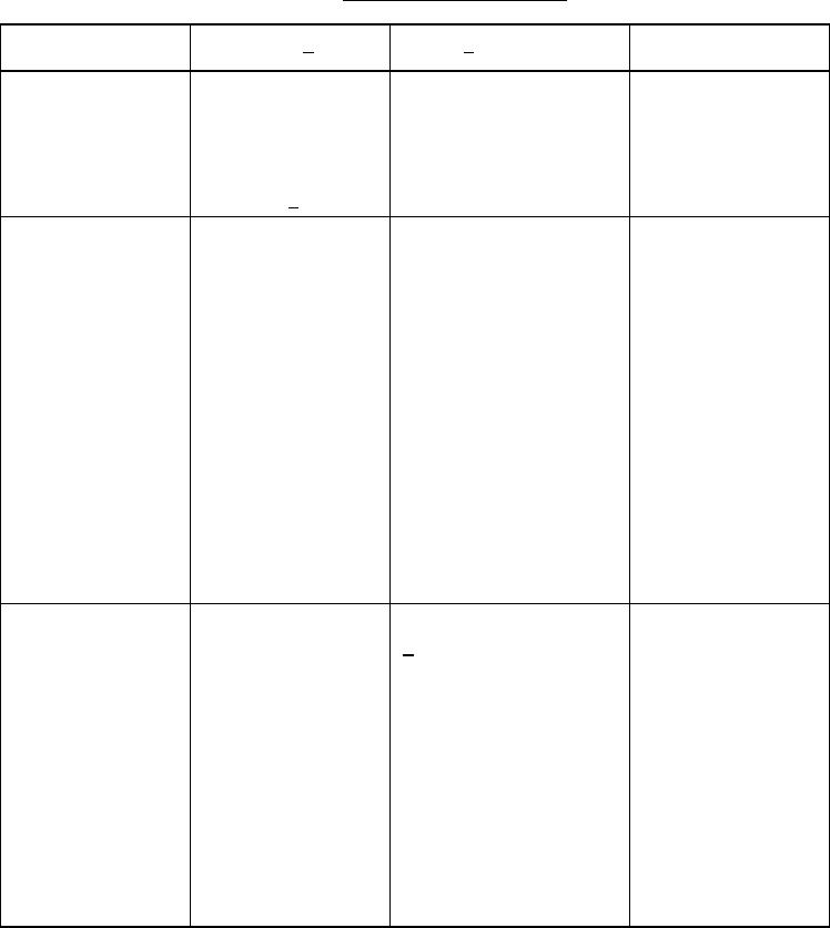
TABLE I. Wafer lot acceptance tests.
Test
Conditions 1/ Limits 3/ Sampling plan
1. Wafer thickness Measurement
shall be performed
after final lap
or polish. All
readings shall be
recorded. 2
/
Maximum deviation of
±2 mil from approved
design nominal 6 mil
minimum.
Two wafers per
lot. Reject lot
if any measurement
exceeds limits or
revert to test of
each wafer.
2. Metallization
thickness
All readings
shall be
recorded.
a. Conductor: 8 kÅ
minimum for single
level metal and for
the top level of
multi-level metal;
5 kÅ minimum for lower
levels, with a maximum
deviation of ±20
percent from the
approved design
nominal.
b. Barrier: Maximum
deviation of ±30
percent from the
approved design
nominal.
One wafer (or
monitor) per lot.
Reject lot if
measurement ex-
ceeds limits or
revert to test
of each wafer.
3. Thermal sta-
bility (ap-
plicable to:
All linear;
all MOS; all
bipolar digi-
tal operating
at 10 V or
more)
Record V
FB
or V
T
.
a. ∆V
FB
or ∆V
T
<
0.75, normalized to
an oxide thickness of
1000Å for bipolar
digital devices oper-
ating at 10 volts or
greater and all
bipolar linear devices
not containing MOS
transistor(s). The
monitor shall have an
oxide and shall be
metallized with the
lot.
One wafer (or
monitor) per lot.
Reject lot if
measurement ex-
ceeds limits or
revert to test
of each wafer.
See footnotes at end of table.
MIL-STD-883F
METHOD 5007.6
19 August 1994
3
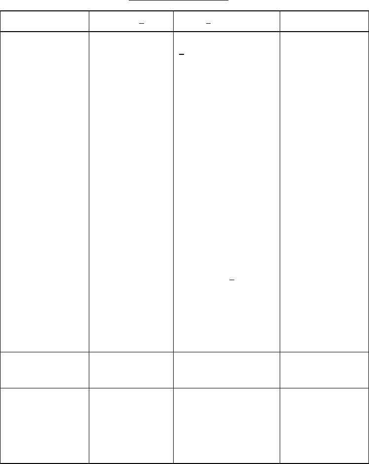
TABLE I. Wafer lot acceptance tests - Continued.
Test
Conditions 1/ Limits 3/ Sampling plan
3. Thermal sta-
bility (ap-
plicable to:
All linear;
all MOS; all
bipolar digi-
tal operating
at 10 V or
more)
Record VFB
or V
T
.
b. ∆V
FB
or ∆
VT
<
1.0 V,normalized to
an oxide thickness of
1,000Å for bipolar
linear devices that
operate above 5 V and
containing MOS tran-
sistor(s), and digital
devices that operate
above 10 V and
containing MOS
structures.
The V
FB
limit shall
not be exceeded by the
sum of the absolute
values of the MOS
oxide transistors and
the metallization ∆.
The monitor(s) shall
be oxidized and
metallized with the
lot. Separate
monitors may be used
for this test.
c. ∆V
FB
or V
T
<0.4 V,
normalized to an oxide
thickness of 1,000Å
for MOS devices. A
monitor consisting of
a gate oxide
metallized with the
lot shall be used.
One wafer (or
monitor) per lot.
Reject lot if
measurement ex-
ceeds limits or
revert to test
of each wafer.
4. SEM MIL-STD-883,
method 2018.
MIL-STD-883,
method 2018.
MIL-STD-883,
method 2018. Lot
acceptance basis.
5. Glassivation
thickness
All readings
shall be
recorded.
6 kÅ minimum for
Si0
2
and 2 kÅ
for Si
3
N
4
with
maximum deviation of
±20 percent from
approved design
nominal.
One wafer (or
monitor) per lot.
Reject lot if any
measurement ex-
ceeds limits
or revert to test
of each wafer.
See footnotes at end of table.
MIL-STD-883F
METHOD 5007.6
19 August 1994
4
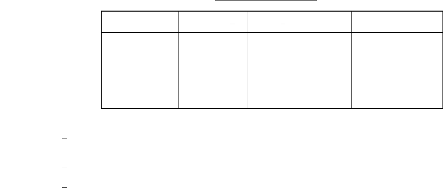
TABLE I. Wafer lot acceptance tests - Continued.
Test
Conditions 1/ Limits 3/ Sampling plan
6. Gold backing
thickness
(when appli-
cable)
All readings
shall be
recorded.
In accordance with
approved design
nominal thickness and
tolerance.
One wafer (or
monitor) per lot.
Reject lot if any
measurement ex-
ceeds limits or
revert to test of
each wafer.
1
/ The manufacturer shall have documented procedures for performing each required test. These procedures shall
be made available to the qualifying activity or acquiring activity upon request.
2
/ This test is not required when the finished wafer design thickness is greater than 10 mil.
3
/ Approved design nominal values or tolerances shall be documented in the manufacturer’s baseline
documentation.
*