MIL- STD-883F 2004 TEST METHOD STANDARD MICROCIRCUITS.pdf - 第519页
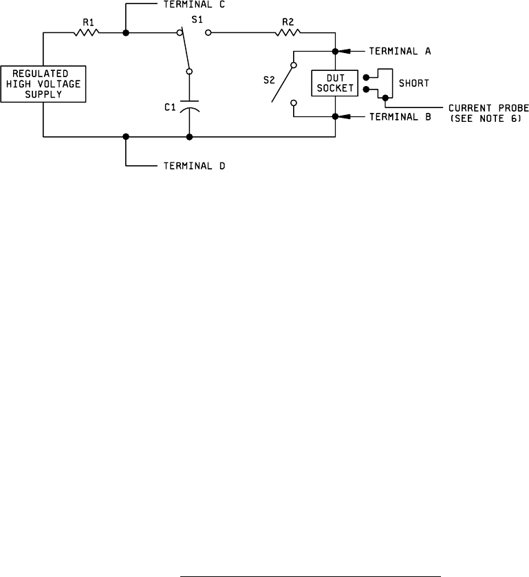
MIL-STD-883F METHOD 3015.7 22 March 1989 5 R1 = 10 6 ohms to 10 7 ohms C1 = 100 picof arads ±10 percent ( Ins ulation r esis tanc e 10 12 ohms minimum) R2 = 1,500 ohms ±1 percent S1 = High volt age relay (Bouncel ess, me…

MIL-STD-883F
METHOD 3015.7
22 March 1989
4
4. SUMMARY. The following details shall be specified in the applicable purchase order or contract, if other than specified
herein.
a. Post test electricals.
b. Special additional or substitute pin combinations, if applicable.
c. Sample size, if other than three devices.
MIL-STD-883F
METHOD 3015.7
22 March 1989
5
R1 = 10
6
ohms to 10
7
ohms
C1 = 100 picofarads ±10 percent (Insulation resistance 10
12
ohms minimum)
R2 = 1,500 ohms ±1 percent
S1 = High voltage relay (Bounceless, mercury wetted, or equivalent)
S2 = Normally closed switch (Open during discharge pulse and capacitance measurement)
NOTES:
1. The performance of this simulator circuit is strongly influenced by parasitics. Capacitances across relays and
resistor terminals, and series inductance in wiring and in all components shall be minimized.
2. As a precaution against transients upon recharge of C1, the supply voltage V
S
may be reduced before switch
S1 is returned to the charging position.
3. Piggybacking DUT sockets is not permitted during verification or classification testing.
4. Switching terminals A and B internal to the simulator to obtain opposite polarity is not recommended.
5. C1 represents the effective capacitance (see 2.3.2).
6. The current probe connection shall be made with double shielded cable into a 50-ohm termination at the
oscilloscope. The cable length shall not exceed 3 feet.
FIGURE 3015-1. EDS classification test circuit (human body model)
.
MIL-STD-883F
METHOD 3015.7
22 March 1989
6
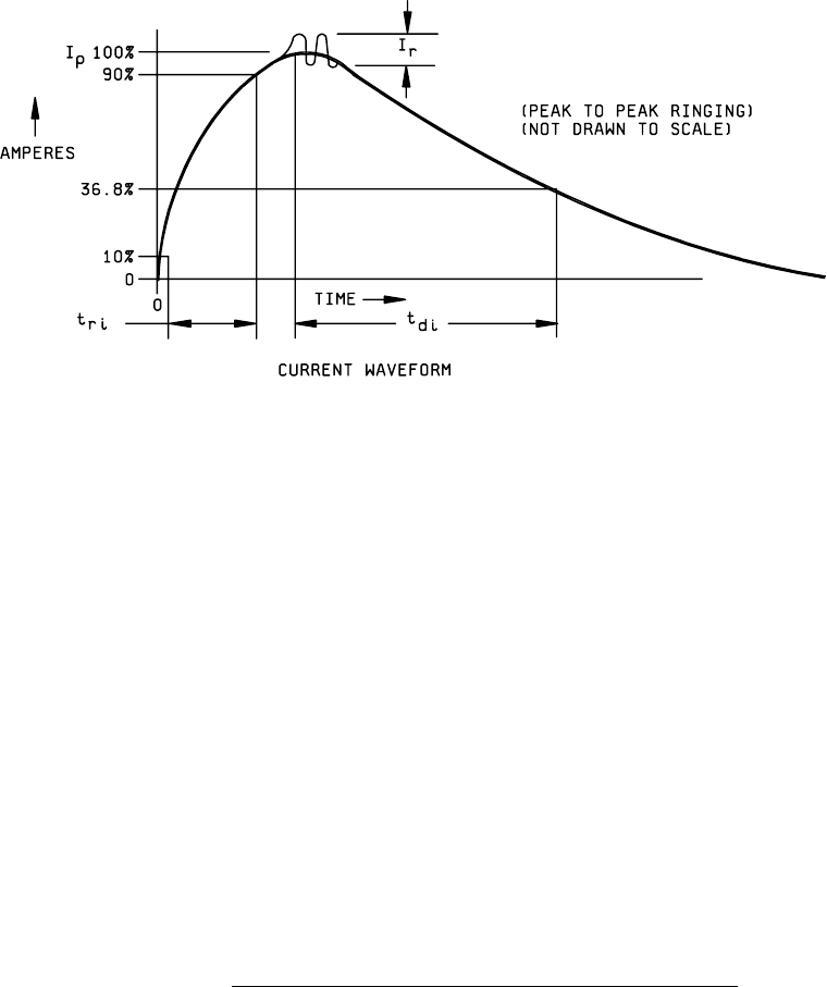
NOTES:
1. The current waveforms shown shall be measured as described in the waveform verification procedure of 3.2,
using equipment meeting the requirements of 2.
2. The current pulse shall have the following characteristics:
Tri (rise time) ---------------Less than 10 nanoseconds.
Tdi (delay time) ------------150 ±20 nanoseconds.
I
p
(peak current) -----------Within ±10 percent of the I
p
value shown in table II for the voltage step selected.
I
r
(ringing) -------------------The decay shall be smooth, with ringing, break points, double time constants or
discontinuities less than 15 percent I
p
maximum, but not observable 100
nanoseconds after start of the pulse.
FIGURE 3015-2. EDS classification test circuit waveforms (human body model)
.