MIL- STD-883F 2004 TEST METHOD STANDARD MICROCIRCUITS.pdf - 第216页
MIL-STD-883F METHOD 2010.11 18 June 2004 6 (30) Passiva tion step . An abr upt change of elevation ( level) of the pas sivat ion suc h as a c ontact window, or operati ng metalli zation c ross over. ( 31) Peri pheral met…
MIL-STD-883F
METHOD 2010.11
18 June 2004
5
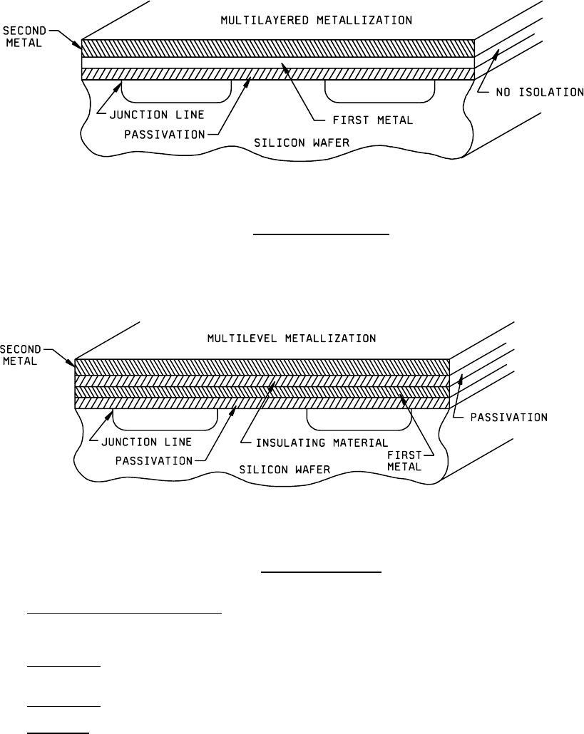
FIGURE 2010-2. Multilayered metallization
.
FIGURE 2010-3. Multilevel metallization
.
(26) Operating metallization (conductors)
. Metal or any other material used for interconnection except metallized
scribe lines, test patterns, unconnected functional circuit elements, unused bonding pads, and identification
markings.
(27) Original width
. The width dimension or distance that would have been present, in the absence of the
observed abnormality (e.g., original metal width, original diffusion width, original beam width, etc.).
(28) Package post
. A generic term used to describe the bonding location on the package.
(29) Passivation
. The silicon oxide, nitride or other insulating material that is grown or deposited directly on the
die prior to the deposition of metal or between metal levels on multilevel devices.

MIL-STD-883F
METHOD 2010.11
18 June 2004
6
(30) Passivation step. An abrupt change of elevation (level) of the passivation such as a contact window, or
operating metallization crossover.
(31) Peripheral metal
. All metal that lies immediately adjacent to or over the scribe grid.
(32) Redistribution Layer (RDL)
. Layer added to original wafer/die surface to allow for the redistribution of bond
pads into a format more suitable to flip chip.
(33) Redistribution metalization
. The metal deposited on the RDL to create the electrical conductors which
connect the original bond pads to the distributed solder bump pads.
(34) Shooting metal
. Metal (e.g., aluminum, gold) expulsion of various shapes and lengths from under the wire
bond at the bonding pad.
(35) Solder ball
. Solder ball or sphere attached to the UBM through the contact via after a re-flow process.
(36) Solder Bump
. Solder that is either electroplated or screened into the photo resist opening. After the photo
resist is removed the solder resembles a bump before it is reflowed into ball or sphere.
(37) Substrate
. The supporting structural material into or upon which or both the passivation, metallization and
circuit elements are placed.
(38) Substrate via
. A small hole formed through the wafer and metallized, causing electrical connection to be
made from the frontside (the side on which the circuitry is formed) to the backside of the wafer.
(39) Thick film
. That conductive/resistive/dielectric system that is a film having greater than 50,000Å thickness.
(40) Thin film
. That conductive/resistive/dielectric system that is a film equal to or less than 50,000Å in thickness.
(41) Under Bump Metalization (UBM)
. Metals deposited on top of the aluminum bond pads or on the solder bump
pads that enhance wetting and protect against intermetalic reactions between the solder and the original
metal on the pads.
(42) Via metallization
. That which connects the metallization of one level to another.
g. Interpretations. Reference herein to "that exhibits" shall be considered satisfied when the visual image or visual
appearance of the device under examination indicates a specific condition is present and shall not require
confirmation by any other method of testing. When other methods of test are to be used for confirming that a
reject condition does not exist, they shall be approved by the acquiring activity. For inspections performed on the
range of 75X to 100X, the criteria of 0.1 mil of passivation, separation or metal can be satisfied by a line of
separation or a line of metal visible.
h. Foreign material control. The manufacturer shall perform an audit on a weekly basis for (1) the presence of
foreign material within incoming piece part lids and bases, and (2) the presence of foreign material on the die
surface or within the package of assembled parts.
The audit of assembled parts may be satisfied during routine internal visual inspection. If the presence of foreign
material is discovered, the manufacturer shall perform the necessary analysis on a sample of the foreign material
on the suspect devices to determine the nature of the material. The manufacturer shall document the results of
this investigation and corrective action to eliminate the foreign material and this information will be available to the
Government QAR, and the acquiring activity or the qualifying activity, as applicable. A corrective action plan shall
be obtained within a maximum of 10 working days of discovery.
The audit of incoming piece part lids and bases shall be performed before parts are assembled, or may be
satisfied during routine incoming quality inspection. If the presence of foreign material of a size 1 mil or greater is
discovered, the manufacturer will analyze the foreign material to determine its nature and document the results of
the analysis. If applicable, these results shall be distributed to the vendor supplying the parts, with the request
that the vendor document corrective actions to minimize or eliminate such foreign material. This information will
be available to the manufacturer, Government QAR, and the acquiring activity or qualifying activity, as applicable.
MIL-STD-883F
METHOD 2010.11
18 June 2004
7
NOTE: The piece part audit requirements can be replaced by a piece part cleaning process, approved by the qualifying
activity, that is always performed either prior to or during the assembly process and these piece parts are stored in a
controlled environment until they are used.
The intent of these procedures is to require investigation and resolution of foreign material problems that do not
have an effective screening or detection methodology but that could cause degradation and eventual failure of the
device function. Repetitive findings without obvious improvements require escalation to Director of Manufacturing
and Director of Quality Assurance to continue processing.
Condition A Condition B
Class level S Class level B
3.1 High power inspection
. Internal visual examination as required in 3.1.1 through 3.1.3 shall be conducted on each
microcircuit. In addition, the applicable criteria contained in 3.1.4 through 3.1.7 shall be used for the appropriate microcircuit
area where glassivation, dielectric isolation or film resistors are used.
NOTE: Unless otherwise specified, for flip chip product the criteria of 3.1 shall apply only to top circuit side inspection. After
die mounting, only criteria in 3.1.3i shall apply.
The high magnification The high magnification
inspection shall be within the inspection shall be within the
range of 100X to 200X. range of 75X to 150X.
For high magnification inspection of GaAs microwave devices, see table I herein. Also, for < 1 micron features, the
manufacturer may implement a sample inspection plan which shall be documented in the manufacturer's internal procedure
and approved by the qualifying activity.
3.1.1 Metallization defects
. No device shall be acceptable that exhibits the following defects in the operating
metallization.
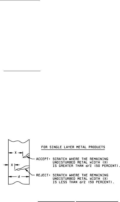
3.1.1.1 Metallization scratches:
a. Scratch in the metallization excluding a. Scratch in the metallization, excluding bonding
bonding pads and beam leads that leaves pads and beam leads, that exposes underlying
less than 50 percent of the original passivation anywhere along its length and leaves
metal width undisturbed (see figure less than 50 percent of the original metal width
2010-4). undisturbed (see figure 2010-5).
NOTE: For GaAs microwave devices, scratches in the gate stripe or gate insertion metallization.
FIGURE 2010-4. Metallization scratch
criteria for class level S.