OM-1461-001_w.pdf - 第8页
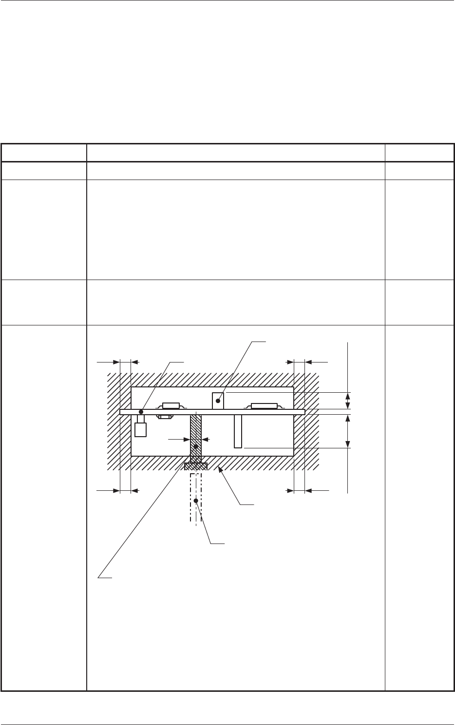
5 3.0 PCB PCB Support Pin (Shows the time of PCB transfer .) Previously-placed Components Unallowed Range Component 3.0 3.0 3.0 F 4 Max. 25.4 PCB Support Pin (Several Places) Notes: (a) The pin can be shifted at "…

Contents
4
Page
0712-001
14. Electrical Circuit Diagram ............................................................... 47
U05 I/O STLT ILB + PWR (L) 1/5 ...................................................... 47
U05 I/O STLT ILB + PWR (L) 3/5 ..................................................... 48
U05 I/O STLT ILB + PWR (R) 1/5 ..................................................... 49
U05 I/O STLT ILB + PWR (R) 3/5 ..................................................... 50
U16 I/O STLT ILB(L) IN ..................................................................... 51
U16 I/O STLT ILB(L) OUT ................................................................. 52
U16 I/O STLT ILB(R) IN .................................................................... 53
U16 I/O STLT ILB (R) OUT ............................................................... 54
Y-Axis (1,2) Motor Circuit Diagram .................................................... 55
Y-Axis (3,4) Motor Circuit Diagram .................................................... 56
X-Axis (1) Motor Circuit Diagram ...................................................... 57
X-Axis (2) Motor Circuit Diagram ..................................................... 58
X-Axis (3) Motor Circuit Diagram ...................................................... 59
X-Axis (4) Motor Circuit Diagram ...................................................... 60
Multi-Functional Head M Circuit Diagram (1) .................................... 61
Multi-Functional Head M Circuit Diagram (2) .................................... 62
Multi-Functional Head M Circuit Diagram (3) .................................... 63
Multi-Functional Head M Circuit Diagram (4) .................................... 64
J28 POWER SUPPLY PCB(1) .......................................................... 65
J28 POWER SUPPLY PCB(2) .......................................................... 66
J28 POWER SUPPLY PCB(3) .......................................................... 67
J28 POWER SUPPLY PCB(4) .......................................................... 68
U171 I/O STLI MF HEAD(1).............................................................. 69
U171 I/O STLI MF HEAD(2).............................................................. 70
U171 I/O STLI MF HEAD(3).............................................................. 71
U171 I/O STLI MF HEAD(4).............................................................. 72
Recognition Unit Connection Diagram 2 ........................................... 73
Recognition Unit Connection Diagram 3 ........................................... 74
Recognition Unit Connection Diagram 4 ........................................... 75
CPU2-L Cable Connection (HLS) ..................................................... 76
CPU2-R Cable Connection (HLS) ..................................................... 77
CPU2-L Cable Connection (SSCNET,AELINK) ................................ 78
CPU2-R Cable Connection (SSCNET,AELINK) ................................ 79
G-SO50-09,10(L) Wiring Material 1 .................................................. 80
G-SO50-09,10(L) Wiring Material 2 ................................................. 81
G-SO50-09,10(L) Wiring Material 3 .................................................. 82
Multi-Functional Head Wiring Block Diagram.................................... 83
5
3.0
PCB
PCB Support Pin
(Shows the time of PCB transfer.)
Previously-placed
Components Unallowed
Range
Component
3.0
3.0 3.0
F4
Max. 25.4
PCB Support Pin (Several Places)
Notes: (a) The pin can be shifted at "20 mm" pitch.
(The shifting is partly possible at "10 mm" pitch.)
(b) Set the support pins such that they do not touch
the already placed components.
(c) The figure shows that the PCB is being supported.
(Front Side of Machine)
Max. 30
1. Scope
0712-001
Unit : mm
1. Scope
This unit manages the multi-functional components in the Direct Drive
Modular Mounter GXH-3 series.
There are three nozzles, placed in series, for each head.
2. Specications
Item Description Special Item
1. Model Name
HM-G300
2. Construction
•Multi-Functional Head : HM-G300
• Multi-Functional Nozzle Stocker : MS-G-300L (For the Blocks 1 and 4)
: MS-G-300R (For the Blocks 2 and 3)
• For attaching to the main body : G-S050-09
(GXH-3 For the Blocks 1 and 4)
: G-S050-10
(GXH-3 For the Blocks 2 and 3)
3. Throughput Chip-Type Components : 24,000 CPH/4 Head
QFP : 20,000 CPH/4 Head
Note
: Excluding the PCB transition time under optimum conditions.
4. Conditions of
PCB before
Placement
(Regulation
of Component
Height)
Note :
The dimensions are those for design reference.
Leave some room for the actual setting.
60712-001
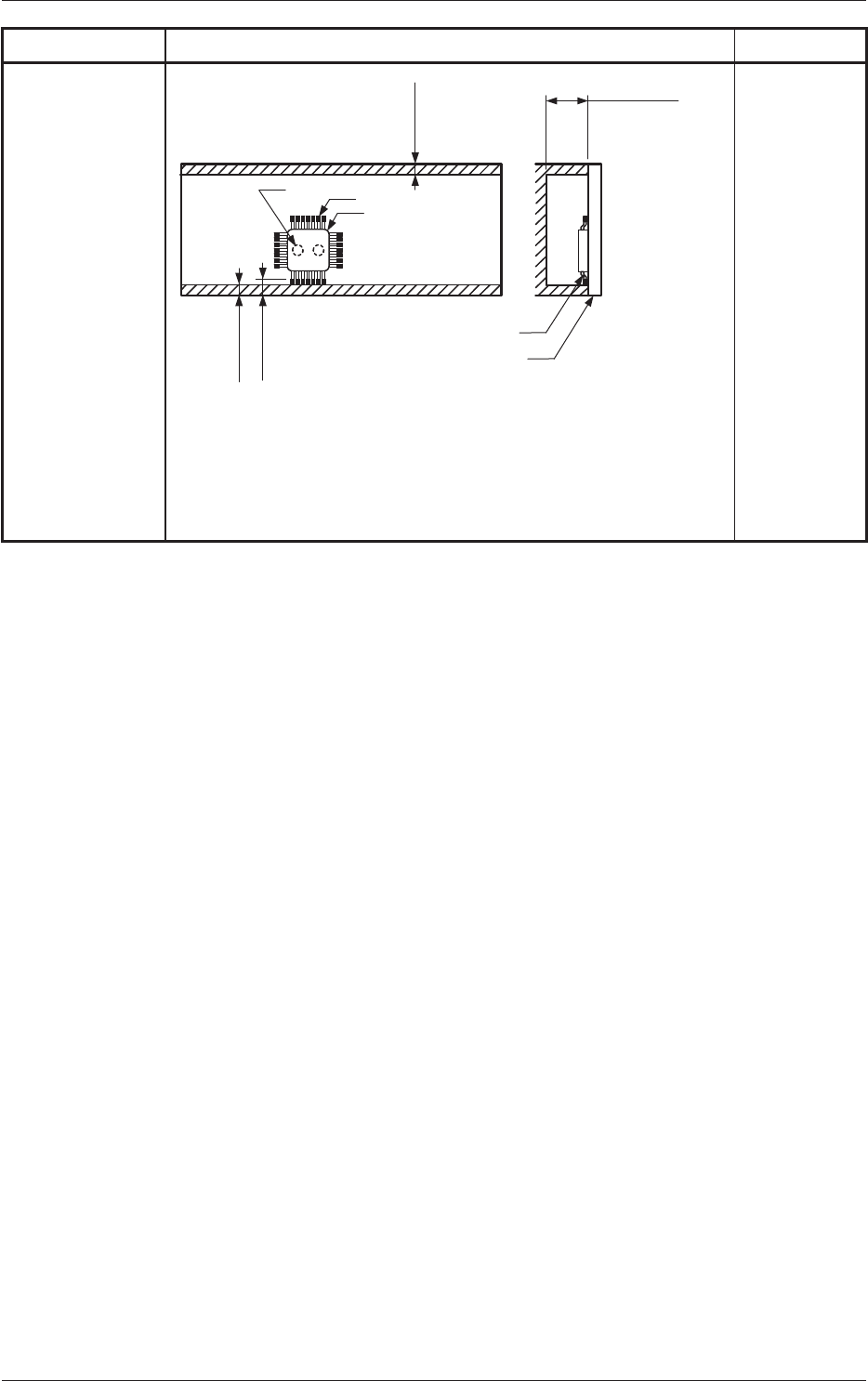
2.Specications
Item Description Special Item
5. Component
Placeable
Range
Unit : mm
Notes :
(a) Theabovegureshowsthatthevacuumnozzlesarenot
protruding from the outer shapes of components.
(b) Components cannot be placed in the shadowed area.
Components cannot be placed in the range (0.5 mm) around
the opening such as a hole.
QFP
Min. 3.5
Min. 3.8
Min. 3.5
Solder Paste
Glue
QFP
PCB
Max. 25.4
Upper
Surface of PCB
(Front Side of Machine)