Specification SIPLACE X-Series规格说明书1.pdf - 第38页
38 Vision Sensor Technology PCB Position Recognition Bad Board Recognition Ink Spot Criteria Methods • Synthetic fiducial recognition method • Mean grayscale value • Histogram method • Template matching Shapes and sizes …

37
Vision Sensor Technology
PCB Position Recognition
Description
Different fiducial shapes
prove to be optimal depend-
ing on the condition of the
surface.
Particularly advisable for
bare copper surfaces with lit-
tle oxidation is the single
cross. Maximum accuracy is
achieved due to the high
information content.
Rectangle, square and circle
are less “informative” but
save space and can even be
used when oxidation is at an
advanced stage. Advisable
for tinned structures are cir-
cle or square because in this
case the ratio of the fiducial
dimensions to the presolder
thickness is particularly
favorable.
Fiducial criteria
Locate 2 fiducials
Locate 3 fiducials
X-/Y-position, rotation angle, mean PCB distortion
in addition: shear, distortion in X- and Y-direction separately
Fiducial shapes Synthetic fiducials: circle, cross, square, rectangle, rhombus,
circular, square, and rectangular contours, double cross, any
pattern
Fiducial surface:
copper
tin
Without oxidation and solder resist
Fiducial warp 1/10 of structure width, both with good con-
trast to environment
Dimensions of synthetic fiducials
min. X/Y size for circle and rectangle: 0.25 mm
min. X/Y size for annulus and rectangle: 0.3 mm
min. X/Y size for cross: 0.3 mm
min. X/Y size for double-cross: 0.5 mm
min. X/Y size for lozenge: 0.35 mm
min. frame width for annulus and rectangle: 0.1 mm
min. bar width / bar distance for cross, double-cross: 0.1 mm
max. X/Y size for fiducial shapes: 3 mm
max. bar width for cross / double-cross: 1.5 mm
min. tolerances, general: 2% of nominal dimension
max. tolerances, general: 20% of nominal dimension
Dimensions of patterns
min. size
max. size
0.5 mm
3 mm
Fiducial environment Clearance around reference fiducial not necessary if there is
no similar fiducial structure in the search area

38
Vision Sensor Technology
PCB Position Recognition
Bad Board Recognition
Ink Spot Criteria
Methods • Synthetic fiducial recognition method
• Mean grayscale value
• Histogram method
• Template matching
Shapes and sizes of fiducials/structures for
synthetic fiducials
other methods
For dimensions of synthetic fiducials,
see page 37
min. 0.3 mm
max. 5 mm
Masking material good coverage
Recognition time depends on the method: 20 ms - 200ms
Description
In the cluster technology
each subpanel is assigned
an ink spot. If this is present
during the measurement via
the PCB vision module, the
corresponding subpanel is
populated.
With this function it is possi-
ble to eliminate costs due to
unnecessary population of
faulty subpanels.
Technical data for PCB position detection
PCB fiducials
Local fiducials
Library memory for recognition
of bad panels
up to 3 (subpanels and multiple panels)
up to 6 for the Long board option (Optional PCB fiducials
are output by the optimization.)
up to 2 per PCB (may be of different type)
up to 255 fiducial types per subpanel
Image analysis Edge detection method (Singular feature) based on gray-
scale values
Lighting method Front lighting
Fiducial recognition time 0.1 s
Field of vision 5.78 x 5.78 mm
39
Vision Sensor Technology
3D Coplanarity Laser Module
Technical data
Components QFP, SO, BGA, gull-wing,
plug
Accuracy
a
a) Per ball / lead.
± 15 µm (3
± 20 µm (4
Max. component size 50 x 50 mm²
Max. connector size 120 x 20 mm²
min. ball diameter / distance 400 µm / 800 µm
Min. number of balls 6
Min. lead width / pitch 300 µm
b
/ 500 µm
b) Please contact your local product manager in the case of
smaller lead widths.
Min. lead number 5
Max.
CO height
17 mm
Positioning option Location 3 on SIPLACE
X2 and X3, alternative to
the 2D coplanarity laser
module
Placement head type TwinHead
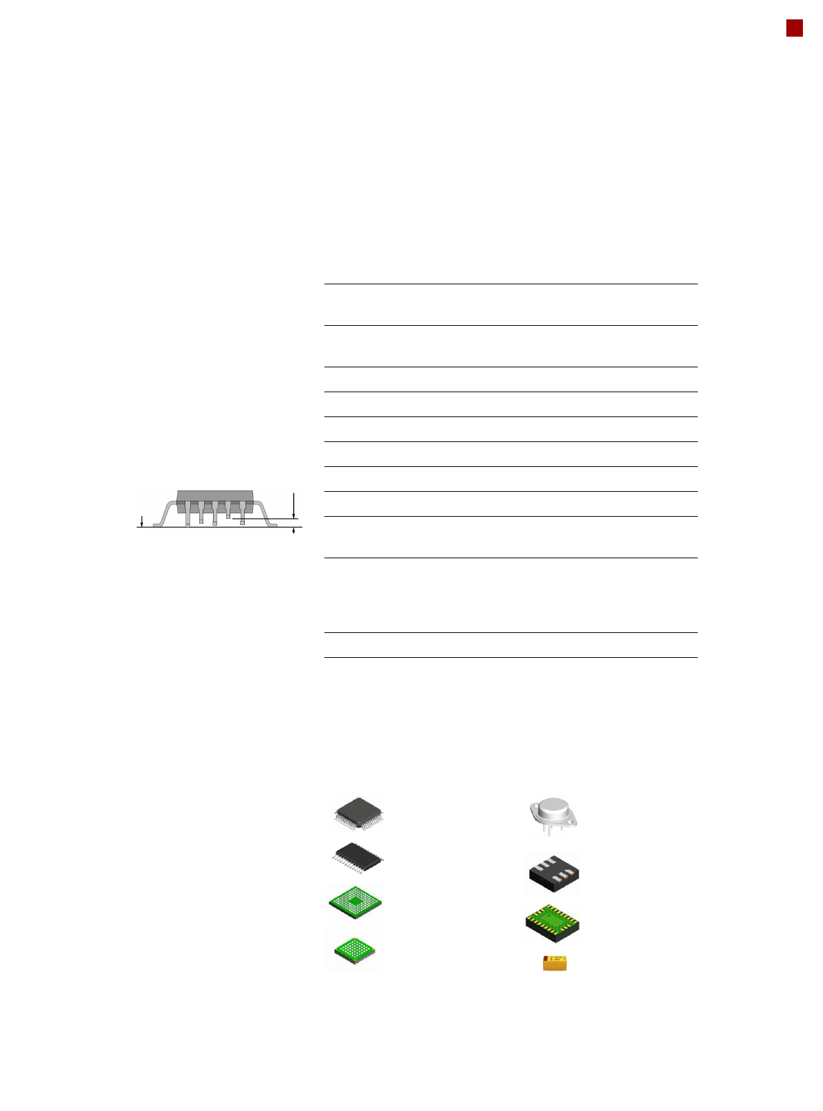
Description
Coplanarity of connections
on a component means that
all connections lie on a level,
the so-called placement
plane. This level is created
from the height information
from the coplanarity mea-
surement. This ensures that
the same soldering condi-
tions apply for all connec-
tions.
Place-
ment
Deviation from
coplanarity
Measuring principle
Measurement of the heights
of the connections occurs
contact-free according to the
principle of laser-triangula-
tion. For the 3D method, a
laser beam line scans the
component. The reflected
light from the laser is repro-
duced on a camera. In this
way the height information
for the connections is
obtained from the reflected
light from the laser.
Restrictions
• Lead or ball recognition
can get worse if the sur-
face is oxidized or glossy.
• The following components
cannot be measured: a
PLCC, SOJ, socket, chip,
bare die, Moulded, Melf,
ECV, DPack, CCGA,
screening plate, compo-
nents with internal con-
nections.
3D coplanarity module
Component inspection possible Component inspection not
possible
Only 5 pins
Lead/ball size within
specification
Also gull-wing
connections
With internal con-
nections, no gull-
wing form
The same applies to screening
plates, plugs with connections
on the underside, bare die etc.