KE-3020_SPE_EN.pdf - 第32页
- 28 - 5.2.11. Coplanari ty (Factor y - Set Option) By moving a tar g et component that is to be measured at constan t speed in the direction (Y - dir ection) perpendicular to the laser line (X - direction), the camera s…
- 27 -
5.2.10. High resolution camera (Factory-Set Option)
When a line unit that permits switching between reflection and transmission recognition and
switching among wavelengths (red, blue, and green) is combined, fine-pitch components
(leads and balls) that cannot be recognized by standard camera can be recognized.
Dimensions of applicable components (Unit: mm)
VCS batch recognition VCS Divided-image recognition
(IC head only)
Reflected-light recognition
component
Pass-through-light recognition
component
Reflected-light recognition component
MNVC: 1.0 x 0.5 to □ 20.0
IC head: □3 to □24.0
MNVC: □ 3.0 to □ 6.0
IC head: □3.0 to □ 24.0
Maximum: 24.0 x 72.0 (at 1x3 division)
□48.0 (at 2x2 division)
* Even though the dimensions exceed □ 20 mm, 24 mm×11 mm is acceptable.
Lead pitch Component height Ball pitch Ball diameter
0.3 to 2.54
- NC specification 0.08 to 12.0
- HC specification 0.08 to 20.0
- EC specification 0.08 to 25.0
0.25 to 2.0 φ0.10 toφ0.63
Lighting
Lead components reflection lighting Coaxial, downward and sideward lighting via red LEDs
Area array components sideward lighting Ball sideward lighting via blue LEDs
Pass-through lighting Profile pass-through lighting via green LEDs
* Adjusting the lighting intensity can be made per component.
- 28 -
5.2.11. Coplanarity (Factory-Set Option)
By moving a target component that is to be measured at constant speed in the direction
(Y-direction) perpendicular to the laser line (X-direction), the camera shoots the diffuse
reflection of laser beam emitted to the component and the device creates 3-D image to
measure displacement without touching the component. This device determines if a
component is appropriate or not based on the 3-D image obtained from the component
information sent by the mounter in advance (that is, checks the height of the electrode).
Colinearity check:
The colinearity check inspects “how much a side on which leads are located is bent in the
up/down directions.”
Coplanarity check:
This check can check coplanarity (uniformity of the bottom of a terminal) of a component with
the three-point method (JEDEC standard: JESD22-B108A) or the method of least squares
(JEDEC standard: JESD22-B108A).
Applicable components
- Components to be recognized with a VCS only.
- BGA, FBGA, connector, and lead components (SOP and QFP) whose respective pitch
is the same and whose respective lead width is the same
-
*1. If you do not enter the correct lead width and electrode size of a component whose
lead width is less than 0.3 mm on the “Component” data screen of the Program Editor,
the system may not be able to detect its terminal correctly.
◆Component height 12.0mm or less (HC spec.:20.0mm、EC spec.:25.0mm)
A product whose laser class is 3b is used in the coplanarity sensor.
- Key switch
The front section of the machine is equipped with a key switch. Only when the key
switch is set to ON, you can use the coplanarity function.
- Cover open
Regardless of the key switch state, any laser is not emitted when the cover opens.
Item
Dimensions
Lead
component
Pitch 0.4 mm or more
Lead width
*1
0.18 mm or more
Lead length 0.3 mm or more
Component size 48 mm×150 mm or less
Ball
component
Pitch 0.8 mm or more
Ball diameter 0.4 mm or more
Component size 48 mm×150 mm or less
- 29 -
5.2.12. Offset Placement After Solder Screen-printing (Factory-Set Option)
A component placement position error may occur after re-flowing if you place a component
on the PWB pad when the solder printing position is shifted from the pad position because a
PWB expands or shrinks.
This function uses an OCC to recognize a gap between a PWB pad and printed solder that is
generated as a result of expansion and/or contraction of a PWB, and places a component on
the printed solder instead of the pad. This makes use of the self-alignment effect to
improve the component placement accuracy after re-flowing.
① Applicable solder shape
A pair of cream solders, which are symmetrical, screen-printed on a PWB pad for a
square chip
* The shape of screen-printed solder should be symmetrical. The system cannot
accurately detect how much to correct the gap unless the shape is symmetrical.
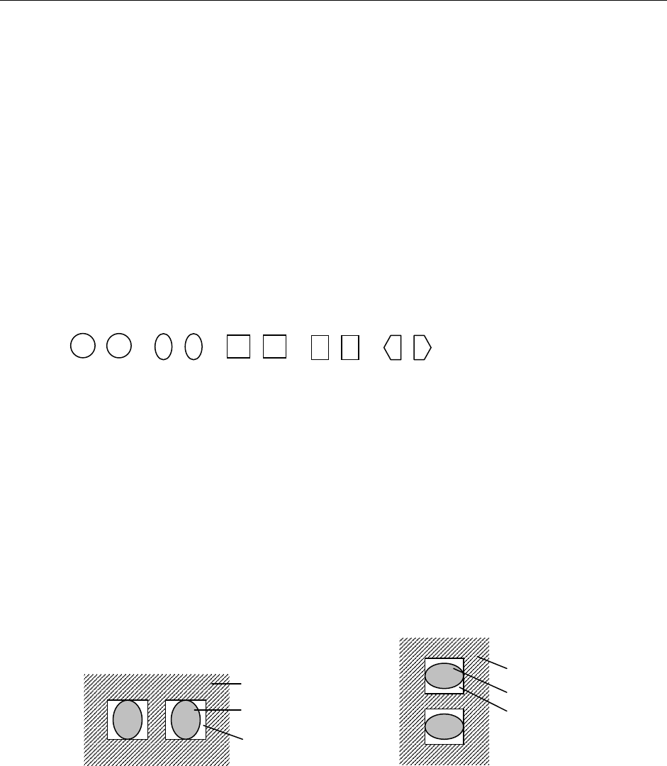
The applicable shapes should be: circle, oval, square, rectangle and pentagon.
(Recognition of other shapes should be checked.)
② Applicable solder
Eutectic solder (NIHON HANDA: RX363-92MY0 (S)) and lead-free solder (TAMURA
KAKEN: TFL-204F-111S)
(* Solder described in parentheses is already checked for its appropriateness.)
③ Applicable chip size
0402, 0603, 1005, 1608, 2012, 3216
* Note that image of a set of solder whose shorter side is 0.16 mm or more and whose
longer side is 3.2 mm or less has to be obtained.
④ Applicable solder angle
0°, 90°, 180°, 270° (Angle error for a camera: within ± 3°)
<Solder angle: 0° or 180°> <Solder angle: 90° or 270°>
⑤ Applicable board material and pad material
− Board material: glass epoxy, paper phenol, flexography, ceramic
− Pad material: gold, copper, hot air leveling
* The solder paste should have a certain level of contrast. If there is a portion whose
brightness is the same as that of solder in the area to be detected due to the condition of the
printed solder, serigraph, a pattern or PWB, and so any image that only solder looks bright
cannot be obtained, the system may not be able to correct the component placement
position by recognizing it. In such a case, you have to set the position of solder paste again
so that it can have the certain level of contrast.
PWB
Solder
Pad
PWB
Solder
Pad