KE-3020_SPE_EN.pdf - 第33页
- 29 - 5.2.12. Offset Place ment After Solder Screen - pr inting ( Factory - Set Option) A component place ment position error may occur after re - flow ing if you place a co mponent on the P W B pad w hen the solder pri…
- 28 -
5.2.11. Coplanarity (Factory-Set Option)
By moving a target component that is to be measured at constant speed in the direction
(Y-direction) perpendicular to the laser line (X-direction), the camera shoots the diffuse
reflection of laser beam emitted to the component and the device creates 3-D image to
measure displacement without touching the component. This device determines if a
component is appropriate or not based on the 3-D image obtained from the component
information sent by the mounter in advance (that is, checks the height of the electrode).
Colinearity check:
The colinearity check inspects “how much a side on which leads are located is bent in the
up/down directions.”
Coplanarity check:
This check can check coplanarity (uniformity of the bottom of a terminal) of a component with
the three-point method (JEDEC standard: JESD22-B108A) or the method of least squares
(JEDEC standard: JESD22-B108A).
Applicable components
- Components to be recognized with a VCS only.
- BGA, FBGA, connector, and lead components (SOP and QFP) whose respective pitch
is the same and whose respective lead width is the same
-
*1. If you do not enter the correct lead width and electrode size of a component whose
lead width is less than 0.3 mm on the “Component” data screen of the Program Editor,
the system may not be able to detect its terminal correctly.
◆Component height 12.0mm or less (HC spec.:20.0mm、EC spec.:25.0mm)
A product whose laser class is 3b is used in the coplanarity sensor.
- Key switch
The front section of the machine is equipped with a key switch. Only when the key
switch is set to ON, you can use the coplanarity function.
- Cover open
Regardless of the key switch state, any laser is not emitted when the cover opens.
Item
Dimensions
Lead
component
Pitch 0.4 mm or more
Lead width
*1
0.18 mm or more
Lead length 0.3 mm or more
Component size 48 mm×150 mm or less
Ball
component
Pitch 0.8 mm or more
Ball diameter 0.4 mm or more
Component size 48 mm×150 mm or less
- 29 -
5.2.12. Offset Placement After Solder Screen-printing (Factory-Set Option)
A component placement position error may occur after re-flowing if you place a component
on the PWB pad when the solder printing position is shifted from the pad position because a
PWB expands or shrinks.
This function uses an OCC to recognize a gap between a PWB pad and printed solder that is
generated as a result of expansion and/or contraction of a PWB, and places a component on
the printed solder instead of the pad. This makes use of the self-alignment effect to
improve the component placement accuracy after re-flowing.
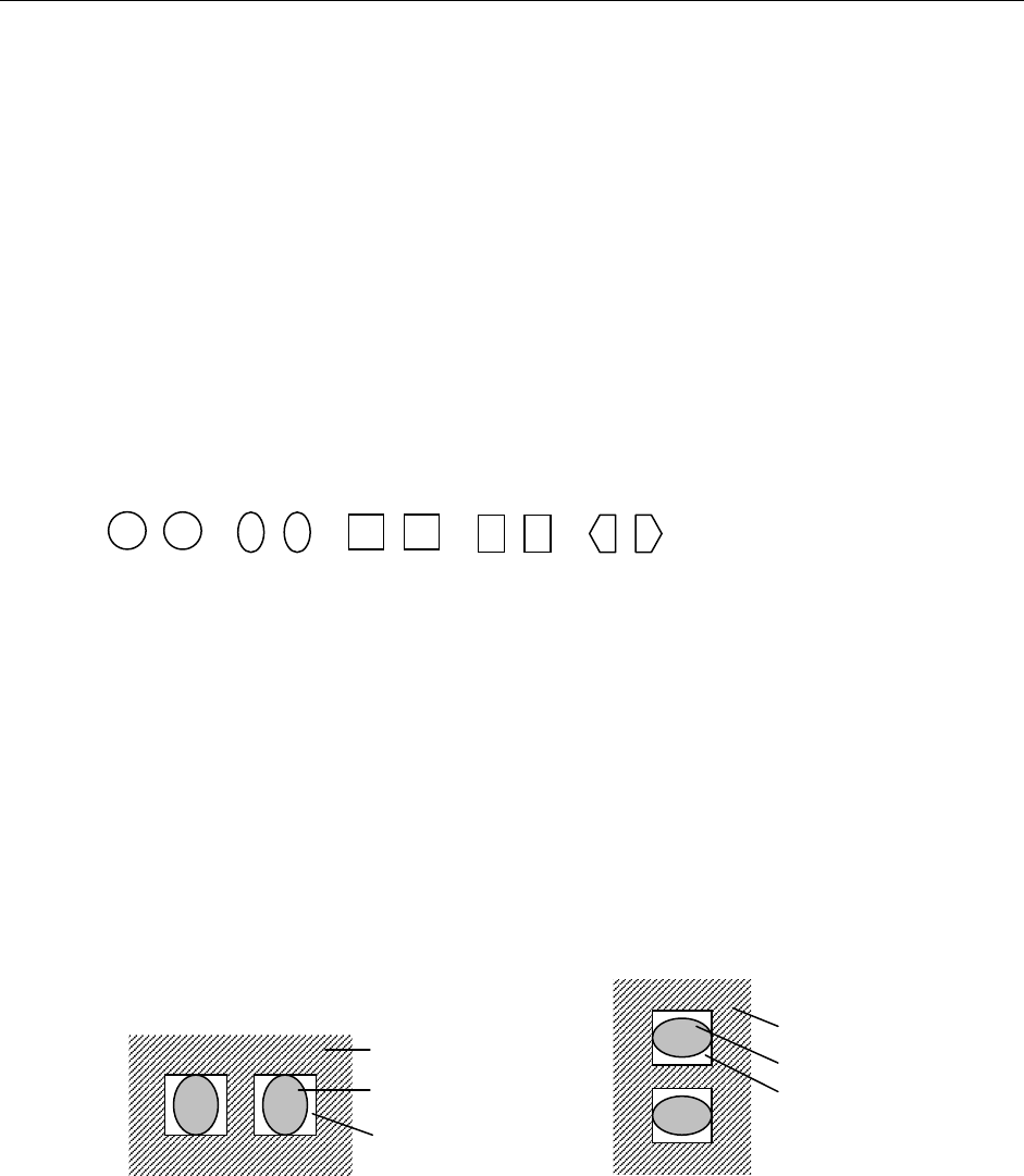
① Applicable solder shape
A pair of cream solders, which are symmetrical, screen-printed on a PWB pad for a
square chip
* The shape of screen-printed solder should be symmetrical. The system cannot
accurately detect how much to correct the gap unless the shape is symmetrical.
The applicable shapes should be: circle, oval, square, rectangle and pentagon.
(Recognition of other shapes should be checked.)
② Applicable solder
Eutectic solder (NIHON HANDA: RX363-92MY0 (S)) and lead-free solder (TAMURA
KAKEN: TFL-204F-111S)
(* Solder described in parentheses is already checked for its appropriateness.)
③ Applicable chip size
0402, 0603, 1005, 1608, 2012, 3216
* Note that image of a set of solder whose shorter side is 0.16 mm or more and whose
longer side is 3.2 mm or less has to be obtained.
④ Applicable solder angle
0°, 90°, 180°, 270° (Angle error for a camera: within ± 3°)
<Solder angle: 0° or 180°> <Solder angle: 90° or 270°>
⑤ Applicable board material and pad material
− Board material: glass epoxy, paper phenol, flexography, ceramic
− Pad material: gold, copper, hot air leveling
* The solder paste should have a certain level of contrast. If there is a portion whose
brightness is the same as that of solder in the area to be detected due to the condition of the
printed solder, serigraph, a pattern or PWB, and so any image that only solder looks bright
cannot be obtained, the system may not be able to correct the component placement
position by recognizing it. In such a case, you have to set the position of solder paste again
so that it can have the certain level of contrast.
PWB
Solder
Pad
PWB
Solder
Pad
- 30 -
5.2.13. Earth Leakage Circuit Breaker (Option to Be Installed at the Factory)
A standard breaker functions if any excess current flows or if a short-circuit fault occurs.
When you replace it with an earth leakage circuit breaker, this new breaker interrupts
electrical leakage, and then prevents the resulting electrical shock, so you can handle the
machine more safely..
5.2.14. Fluxer (Option to Be Installed at the Factory)
This is a flux supply device that applies flux to ball components such as a BGA, CSP and flip
chip (does not apply any adhesive or solder paste).
You can install this device on the mounter with either of the following two methods.
<Where to install>
Installation position
Remarks
Rear bank The number of components to be supplied onto the rear bank is restricted
Mechanical bank
The area for twelve mechanical 8-mm tape feeders is to be occupied.
(A connector bracket option is required separately.)
Electric bank The area for six electric 8-mm tape feeders is to be occupied.
Base frame
Any MTC cannot be installed on the bank at the same time.
Supply of components onto the rear bank is not restricted at all.
*The type of attached on an electric bank does not correspond to the Feeder exchange trolley RF.
<Facility specifications>
Item
Specifications
Remarks
1
Applicable flux viscosity
8.4 Pa·s to 22.0 Pa·s
2
Cycle time required for flux
application and component
placement
1,100cph
When the distance each of the X and
Y axes travels is 450 mm or less
3
Cavity
dimensions
(*See Note 3.)
Depth
Minimum 0.02 mm (± 5 μm)
Maximum 0.2 mm (± 10 %)
Size
Maximum 30 mm×30 mm
(*See Note1 and 2.)
Maximum size of a cavity when only
one cavity is provided
Number
of cavities
1 to 4
Maximum eight on the top and
bottom sides
4
Power consumption
24 VDC/0.3 A
5
Life
5 years
(22 hours×300 days)/1 year
6
Parts needing periodic
replacements
Electromagnetic valve, cylinder
Time for replacement:
2 years after use
7
Consumables
Fluxer plate, flux container
Time for replacement:
1 year after use
Note 1: The cavity size shall be “the maximum size of a component to be used” + “3-mm
margin around the component.”
Note 2: When two or more cavities are used, all cavities shall fit in the 30 mm×30 mm
area.
Note 3: If you need a cavity whose dimensions are not any of the JUKI standard
dimensions, contact our Sales person.
Standard part
Part number
Dimensions of a cavity
Fluxer plate 120/200
40044090
Size: X = 30 mm, Y = 30 mm
Depth: Front 0.12 mm/Rear 0.20 mm
Fluxer plate 30/50/70/100
40044091
Size: X = 30 mm, Y = 14 mm
Depth: Front A 0.03 mm/Front B 0.05 mm
Rear A 0.10 mm/Rear B 0.07 mm