KE2040Instruction Manual Ver2.01,REV04.2003.6.25.pdf - 第36页
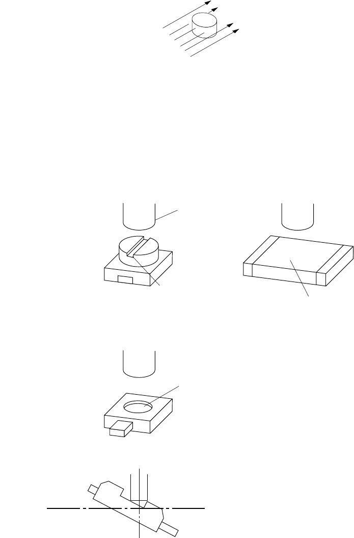
1 − 19 Note: For the shape of chip component s to be mounted (1) For the part s whose shape is cylindrical, there is no minimum shade when turned, and chip recognit ion by laser align is ther efor e impossible. (2) A poo…
1 − 18
Component Name Shape
MNLA
*1
FMLA Standard
VCS
Optional
VCS-1
Optional
VCS-2
Optional
VCS-3
Package
Pitch: 0.65 or more
Dimensions: 20 mm x 20 mm or
less, or 23.5 mm (length) x 11 mm
(width) or less
Recognizable with laser
○
○ ○
Pitch: 0.65 or more
Dimensions: 20 mm x 20 mm or
less, or 23.5 mm (length) x 11 mm
(width) or more but 33.5 mm x 33.5
mm or less
Recognizable with laser
○ ○
Pitch: 0.4 or more
Dimensions: 150 mm x 150 mm or
less
Recognizable with the VCS
○
Pitch: 0.3
Dimensions: more than 24 mm x
24 mm, but 33.5 mm x 33.5 mm or
less
Recognizable with the VCS
○
Pitch: 0.3
Dimensions: more than 16 mm x
16 mm, but 24 mm x 24 mm or less
Recognizable with the VCS
○ ○
Unidirectional lead
connector
Bidirectional lead
connector
Pitch: 0.3
Dimensions: 16 mm x 16 mm or
less
Recognizable with the VCS
○ ○ ○
Pitch: 0.65 or more
Dimensions: 20 mm x 20 mm or
less, or 23.5 mm (length) x 11 mm
(width) or less
Recognizable with laser
○
○ ○
Pitch: 0.65 or more
Dimensions: 20 mm x 20 mm or
less, or 23.5 mm (length) x 11 mm
(width) or more but 33.5 mm x 33.5
mm or less
Recognizable with laser
○ ○
Pitch: 0.5 or more
Dimensions: 150 mm x 150 mm or
less
Recognizable with the VCS
○
Pitch: 0.3
Dimensions: more than 24 mm x
24 mm, but 33.5 mm x 33.5 mm or
less
Recognizable with the VCS
○
Pitch: 0.3
Dimensions: more than 16 mm x
16 mm, but 24 mm x 24 mm or less
Recognizable with the VCS
○ ○
IC socket
Pitch: 0.3
Dimensions: 16 mm x 16 mm or
less
Recognizable with the VCS
○ ○ ○
Dimensions: more than 24 mm x
24 mm, but 33.5 mm x 33.5 mm or
less
○
Dimensions: more than 16 mm x
16 mm, but 24 mm x 24 mm or less
○ ○
FBGA
Dimensions: 216 mm x 16 mm or
less
○ ○ ○
Tape
Stick
Tray
*1 : applicable to a KE-2020
1 − 19
Note: For the shape of chip components to be mounted
(1) For the parts whose shape is cylindrical, there is no minimum shade when turned,
and chip recognition by laser align is therefore impossible.
(2) A poor pickup or placement accuracy could result if the top surface of the
component to be placed is curved, protruded, or dented. Avoid using such
components. (Some such components may, however, be handled by changing
the nozzle number.)
<Typical pickup failures>
MO
MO
<Typical poor placement accuracy>
Pickup nozzle
Slotted groove
Embossed characters
Dented
Laser recognition
1 − 20
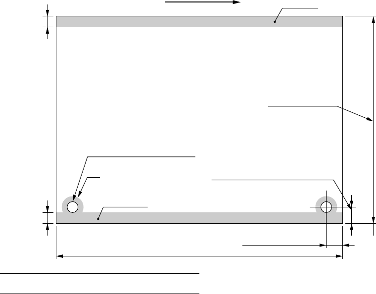
1.1.7 Printed circuit board specifications
1. Board size
Min. : X 50 mm x Y 30 mm
Note that the minimum size becomes 50 mm x 50 mm (X/Y) (optional)
when the machine is equipped with the automatic PWB width
adjustment function.
Max. : [KE-2040M] X 330 mm x Y 250 mm
[KE-2040L] X 410 mm x Y 360 mm
[KE-2040E] X 510 mm x Y 460 mm
X : Along the movement of the board
Y : From front to rear (and reversely) of the machine
2. Board thickness
Min. : 0.4 mm
Max. : 4 mm
3. Board warp limit
0.2 mm or less per 50 mm
1 mm or less both for upward and downward directions
(Conforms to JIS B 8641.)
4. Board limitations
(1) Marginal area
3
3
Note: Dimension at the factory
Movement of PWB
Marginal area
Standard φ4
+0.1
mm
0
φ2.5 - φ4
+0.1
mm (Optional)
0
[KE-2040M] 30 - 250mm
[KE-2040L] 30 - 360mm
[KE-2040E] 30 - 460mm
5 ± 0.1mm
5 - 7mm for particular ordering (factory-set)
Marginal area
Conveying rail (fixed)
Standard 5 ± 0.1mm (Note)
[KE-2040M] 50 - 330mm, [KE-2040L] 50 - 410mm, [KE-2040E] 50 -510mm