00198375-02_UM_OnBoardPCB-Inspection-R18-1_DE_EN.pdf - 第43页
2 What is Onboard PCB Inspection? 2.4 Prerequisites and Restrictions User Manual / Bedienungsanleitung Onboard PCB Inspection 06/2018 43 2.4.2 Regarding Solder Paste Inspection (SPI) NOTICE No complete substitute for SPI…
2 What is Onboard PCB Inspection?
2.3 The Inspection Methods
42 User Manual / Bedienungsanleitung Onboard PCB Inspection 06/2018
2.3 The Inspection Methods
2.3.1 Solder Paste Inspection (SPI)
This inspection method checks the quality of the solder paste which has been applied. The solder
paste in the component placement area is inspected before placement.
●
Both the solder volume and the average solder height are inspected.
●
Clearly detectable solder bridges are recognized.
●
The inspection is performed in the first machine of the line.
2.3.2 Before Placement Inspection (BPI)
This inspection method checks whether the previously placed components are missing at the
placement position or whether lost components are present there. This is particularly useful for
BGA, LGA or QFP components and also for shields.
Application cases for component types
●
The main use case is to check if all components are present. Whether components are placed
with an offset, is only detected for large offsets (however, this inspection method is no meas-
uring tool for checking the placement accuracy).
●
Before a BGA, an LGA or QFP component is placed, an inspection can be performed to make
sure that no other component or foreign body is on or next to the solder deposits. This en-
sures that the BGA balls are placed directly onto the solder pads.
●
Before a shield is placed over components, an inspection is performed to make sure that
these previously placed components are already present in the correct places (under the
shield).
2.3.3 After Placement Inspection (API)
This inspection method checks whether the component has been correctly placed.
●
Components which have already been placed will be inspected to see if they have been cor-
rectly placed in the right position.
2.4 Prerequisites and Restrictions
2.4.1 General Notes
●
In exceptional cases, you may need to repeat the teaching process, if the appearance of the
placed boards, the solder paste pressure etc. has changed significantly from the original
teaching result. The better the teached reference image is, the better will be the result later
on.
●
Pseudo errors could occur as an exception. This is mainly the case if shadowing effects occur
i.e. if components are placed too close to each other or if relatively high components have
been placed already.
NOTICE
Recognition performance depends on the actual use case
The recognition performance depends on the actual use case. That means you always
have to check and decide for the actual case how good the procedure works. In unfavor-
able cases, an increased "error alarm" rate or some not recognized "lost components" can
be expected. A 100% security is not guaranteed.
●
The placement positions to be inspected must have an angle which is a multiple of 90°.
2 What is Onboard PCB Inspection?
2.4 Prerequisites and Restrictions
User Manual / Bedienungsanleitung Onboard PCB Inspection 06/2018 43
2.4.2 Regarding Solder Paste Inspection (SPI)
NOTICE
No complete substitute for SPI-AOI
The Solder Paste Inspection is not a complete substitute for SPI-AOI. It only produces a
good/bad result.
Restrictions
●
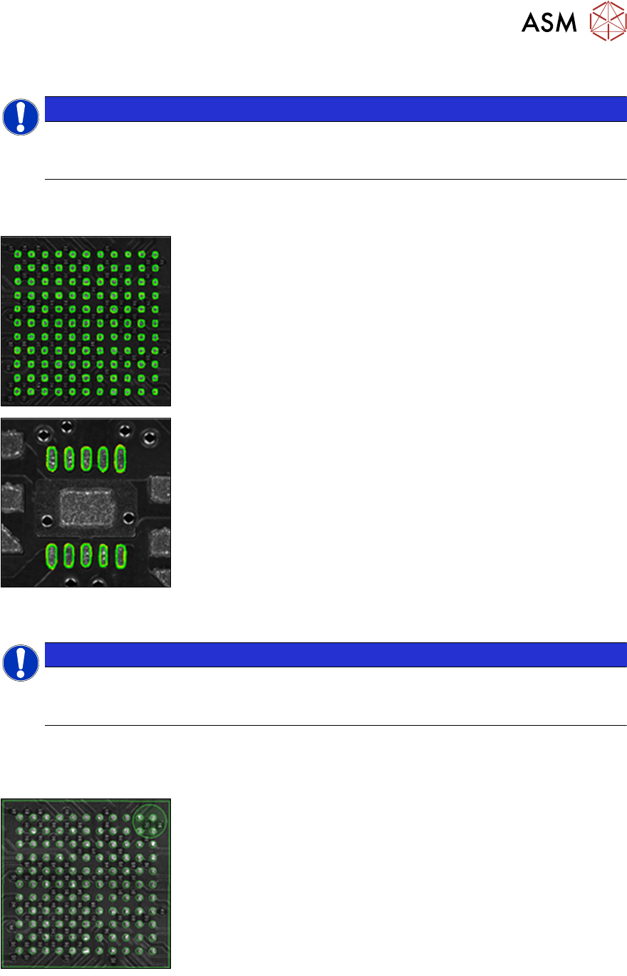
No offsets are recognized or only clear solder bridges are recognized.
Prerequisites for BGA:
●
The diameter of solder pads must be ≥ 0.15 mm.
Prerequisites for "non"BGAs:
●
The solder pads must have a pitch of ≥ 0.4mm.
2.4.3 Regarding Before Placement Inspection (BPI)
NOTICE
The offset inspection only permits a good/bad result.
The offset inspection only permits a good/bad result. This is not proof of placement accur-
acy.
General Requirements
●
The smaller the process variations during solder paste printing are, the less is the pseudo er-
ror rate. The pseudo error rate is higher in the case of greater process variations.
Prerequisites for BGA, LGA or QFP components:
●
Lost components are only recognized reliably up to a MINIMUM
size of 0201.
2 What is Onboard PCB Inspection?
2.4 Prerequisites and Restrictions
44 User Manual / Bedienungsanleitung Onboard PCB Inspection 06/2018
Prerequisites for shields:
●
There must be enough space between the components already
placed (general rule is approx. a space equal to the height of the
component around the components). Otherwise, there is the
danger of a reduced performance in the recognition of lost com-
ponents (both increased "false alarms" and "missed defects").
●
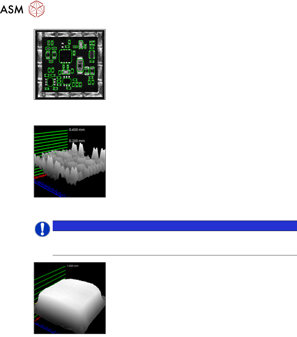
The permissible height of the components already placed is <
1mm.
●
Components which are only partly inside the inspection area are
NOT permitted.
●
Lost components are only recognized reliably up to a MINIMUM
size of 0201.
●
The permissible height of the components already placed is less
than 1 mm.
●
The smallest component size which can be inspected is the
0201.
This image shows a height profile in which the height of all compon-
ents is significantly less than 1 mm.
2.4.4 Regarding After Placement Inspection (API)
NOTICE
The offset inspection only permits a good/bad result.
The offset inspection only permits a good/bad result. This is not proof of placement accur-
acy.
Prerequisites:
●
The permissible height of the components already placed is <
1mm.
●
The smallest component size which can be inspected is the
0201.