00198375-02_UM_OnBoardPCB-Inspection-R18-1_DE_EN.pdf - 第52页
4 Teaching Inspection Areas at the Station 4.2 Teaching Solder Paste Inspection (SPI) 52 User Manual / Bedienungsanleitung Onboard PCB Inspection 06/2018 4.2.2 Inspecting the Solder Deposit Teaching Area The area to be i…
4 Teaching Inspection Areas at the Station
4.2 Teaching Solder Paste Inspection (SPI)
User Manual / Bedienungsanleitung Onboard PCB Inspection 06/2018 51
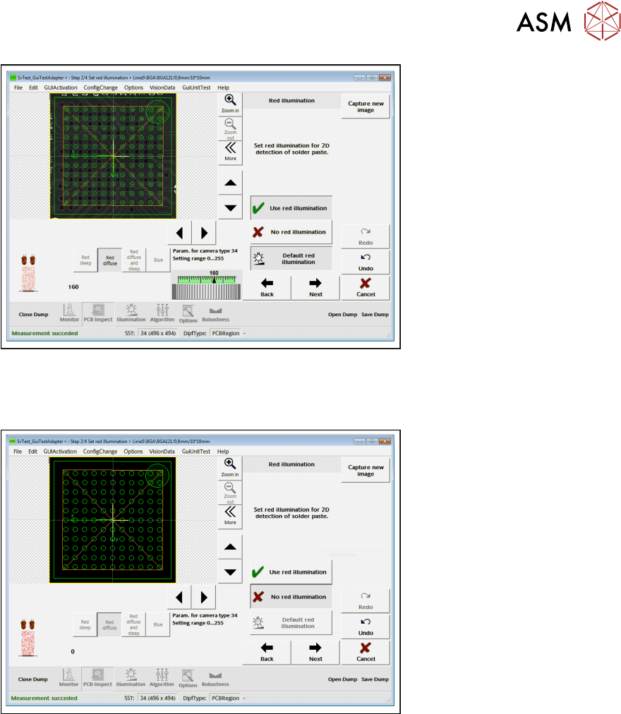
► Select Use red illumination and click on Next.
Switching off the red lighting
► Select No red illumination to switch off the red lighting.
► Click on the Next button.
4 Teaching Inspection Areas at the Station
4.2 Teaching Solder Paste Inspection (SPI)
52 User Manual / Bedienungsanleitung Onboard PCB Inspection 06/2018
4.2.2 Inspecting the Solder Deposit Teaching Area
The area to be inspected and in which the solder deposits are located, needs to be defined. This
area must be defined for the teaching procedure. The solder deposits in this taught area will then
be inspected at the station.
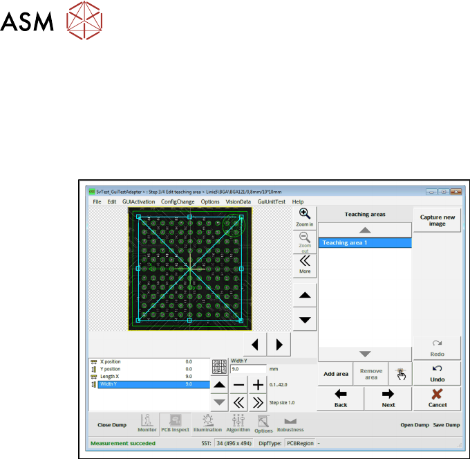
As a default a teaching area has already been defined for each lead group in the component de-
scription. The example shows all the ball leads for a BGA.
As a rule, you will not need to add another teaching area. However, check the position and size of
the teaching area to make sure.
●
Area with green border = component description
●
Area with light blue border = the teaching area currently selected
The defined teaching areas can be selected at Teaching areas.
For further information please refer also to the Online Help.
Tips and tricks
●
The teaching area (light blue border) should be slightly bigger than the area with the solder
deposits actually is.
●
You may need to move the teaching area so that all the solder deposits can be reached.
●
Only define the solder deposit area as the teaching area. For example, four teaching areas for
QFPs (a separate teaching area per connection group).
●
When using larger QFPs, you may find that not all the solder deposits are completely visible
on the first teaching run.
– Solution: increase the teaching area accordingly and take another image.
► Click on the Next button.
4 Teaching Inspection Areas at the Station
4.2 Teaching Solder Paste Inspection (SPI)
User Manual / Bedienungsanleitung Onboard PCB Inspection 06/2018 53
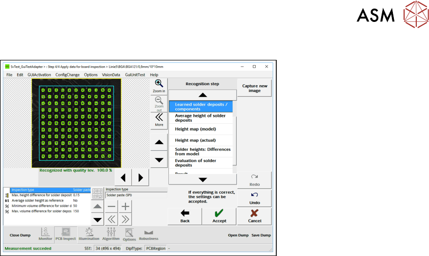
ð The model is taught internally. The result of this procedure is shown below.
► Go to Recognition step and click on Learned solder deposits/components.
ð All successfully recognized solder deposits will be marked with a green border.
Tips and tricks
If not all of the solder deposits to be inspected are marked with a green border, you will need to
teach again. Select stronger lighting, correct the teaching areas and repeat the procedure.
Parameters
Various parameters can be set to improve the result.
●
Inspection type
– Shows the setting of the inspection type in SIPLACE Pro for your information.
●
Max. height difference for solder deposit
– The maximum value by which the measured solder height (average value of all height val-
ues of a solder deposit) may deviate from the target value.
●
Solder height average value as reference
– If No is selected, for example, a separate average solder height is calculated for each
solder deposit. Each solder deposit has its own target values during the inspection then.
– If Yes is selected, there are common target values. For the "average solder height" the
(common) target value is calculated from the average value (average of the average solder
height of all teached deposits).
●
Min. volume difference for solder deposit
– Lower threshold value of the solder volume (in % of the target value)
●
Max. volume difference for solder deposit
– Upper threshold value of the solder volume (in % of the target value)
4.2.3 Evaluating the Teaching Result
Here, you see the inspection result. If defects are already detected here, teach again with a better
sample PCB.
4.2.3.1 Evaluating the solder deposit
After teaching the model, a test inspection is automatically started with the current model.
To view the test inspection result, go to Monitor => Recognition step => Evaluation of solder
deposits.