00198375-02_UM_OnBoardPCB-Inspection-R18-1_DE_EN.pdf - 第61页
5 Inspection Process at the Station 5.1 Successful Inspection Results User Manual / Bedienungsanleitung Onboard PCB Inspection 06/2018 61 5 Inspection Process at the Station 5.1 Successful Inspection Results If the inspe…
4 Teaching Inspection Areas at the Station
4.4 Teaching with After Placement Inspection
60 User Manual / Bedienungsanleitung Onboard PCB Inspection 06/2018
Tips and tricks
●
During the teaching procedure and directly afterwards, an inspection will be performed with
the model which has just been inspected. These results can also be selected in the Recogni-
tion step list and will be shown in the image view.
– Result of component presence inspection
– Lost components (grayscale image)
●
Only those components which were recognized during teaching will be checked for presence.
If a component to be checked is not marked with a blue border here, it was not found.
– If defects are already detected here, teach again with a better sample PCB.
– Select stronger lighting, correct the teaching areas and repeat the procedure.
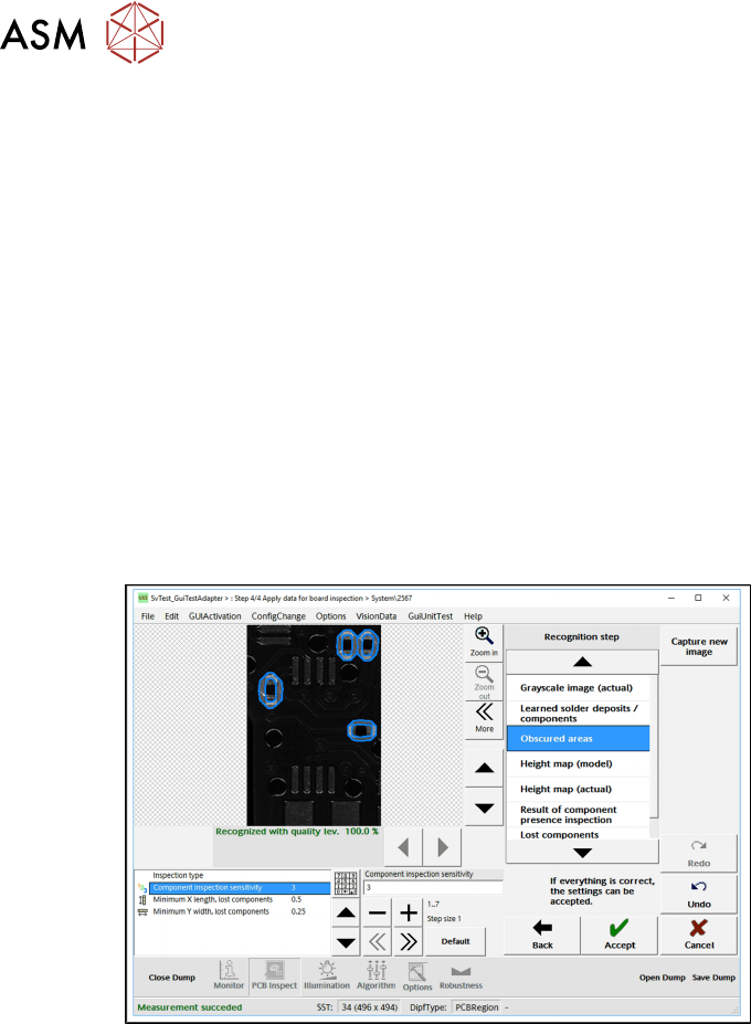
4.3.4.1 Checking Obscured Areas
Here, all areas that are obscured by a teached component are highlighted. If more components
that were not teached are located in these areas, these were not teached because they are ob-
scured.
► Go to Recognition step and select Obscured areas.
4.4 Teaching with After Placement Inspection
The teaching procedure for After Placement Inspection (API) is the same as that for Before Place-
ment Inspection (BPI).
Tips and tricks
●
When teaching with After Placement Inspection (API), we advise using only one teaching
area. The component which has just been placed should be fully covered by this area.
5 Inspection Process at the Station
5.1 Successful Inspection Results
User Manual / Bedienungsanleitung Onboard PCB Inspection 06/2018 61
5 Inspection Process at the Station
5.1 Successful Inspection Results
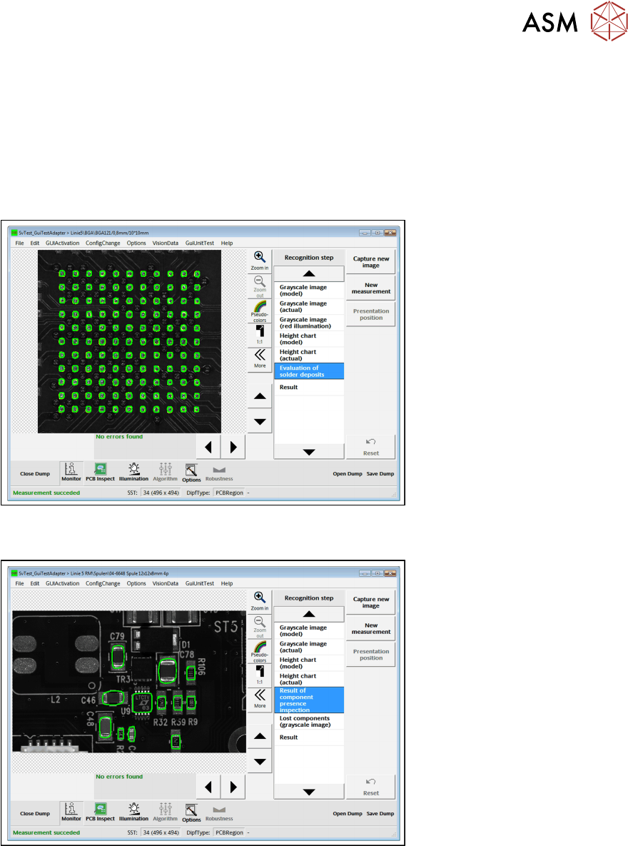
If the inspection was completed successfully, the relevant dialog will be shown. A few examples of
successful inspection results are shown below.
Good example for successful solder paste inspection
Good example for successful inspection of components before placement (required
components are present)
5 Inspection Process at the Station
5.2 Comparing Solder Height Differences From Model
62 User Manual / Bedienungsanleitung Onboard PCB Inspection 06/2018
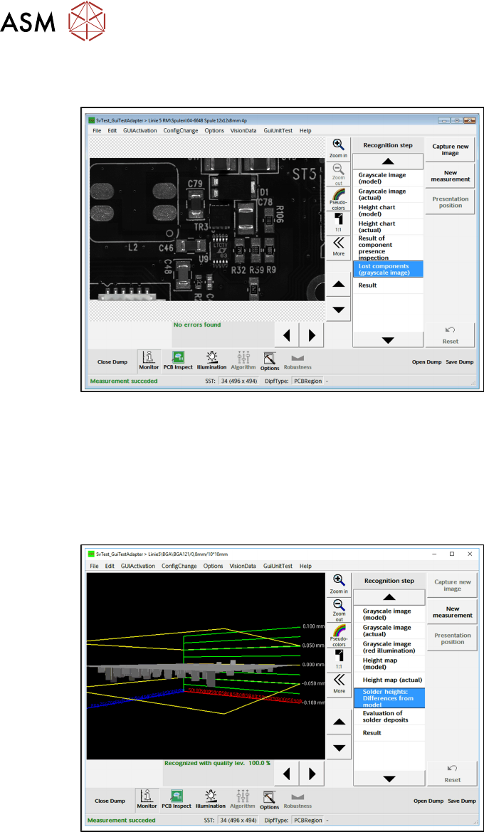
Good example for successful inspection of components after placement (no lost
components found)
Good example
5.2 Comparing Solder Height Differences From Model
Here, a 3D view indicates for each solder deposit how strong its calculated average solder height
deviates from the reference value (model). The borders are shown as yellow rectangles at the cor-
responding Z position.
► Go to Recognition step and select Solder heights: differences from model.
5.3 Handling of Bad Inspection Results
5.3.1 Compare solder deposits
If errors occur, solder deposits can be compared. In the example, the reference image is compared
with the actual image of the solder pad. The diagram shows the difference and reports if the solder
volume is too low.
► Go to Recognition step and select Solder defect comparison# xxx.