00198375-02_UM_OnBoardPCB-Inspection-R18-1_DE_EN.pdf - 第50页
4 Teaching Inspection Areas at the Station 4.2 Teaching Solder Paste Inspection (SPI) 50 User Manual / Bedienungsanleitung Onboard PCB Inspection 06/2018 4.2 Teaching Solder Paste Inspection (SPI) You need to define the …
4 Teaching Inspection Areas at the Station
4.1 Teaching Required
User Manual / Bedienungsanleitung Onboard PCB Inspection 06/2018 49
4 Teaching Inspection Areas at the Station
When the recipe data with the enabled inspection options are downloaded for the first time to the
station, you will need to teach the areas of the individual placement positions. Reference images of
the PCB areas to be inspected are acquired. These images are used to create the inspection
model. Take care during teaching to ensure an inspection as robust as possible. This reference
(target state) is then compared to the actual state of the placement positions to be inspected, dur-
ing the placement process. If both states match, placement will be performed. If they do not match,
placement will be stopped with a detailed error message and the operator will need to take action.
4.1 Teaching Required
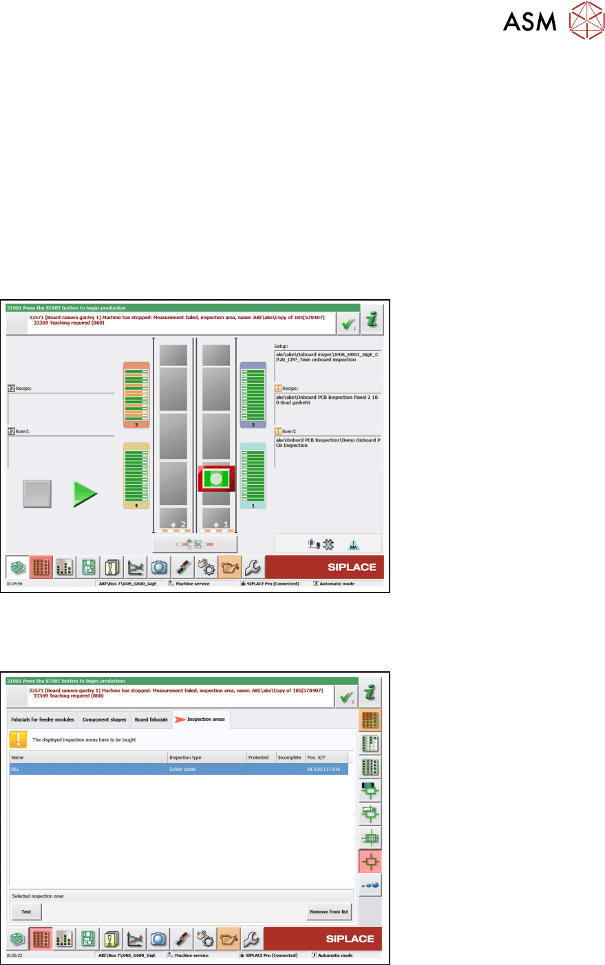
If there is no teaching data present at the station or if the teaching data are faulty, the machine will
be stopped and the Teaching required error message will be shown.
► Select the teaching menu.
ð The teaching view shown varies according to the inspection type chosen.
Example of Solder Paste Inspection (SPI)
4 Teaching Inspection Areas at the Station
4.2 Teaching Solder Paste Inspection (SPI)
50 User Manual / Bedienungsanleitung Onboard PCB Inspection 06/2018
4.2 Teaching Solder Paste Inspection (SPI)
You need to define the area with the solder deposits to be inspected.
4.2.1 Setting the Illumination.
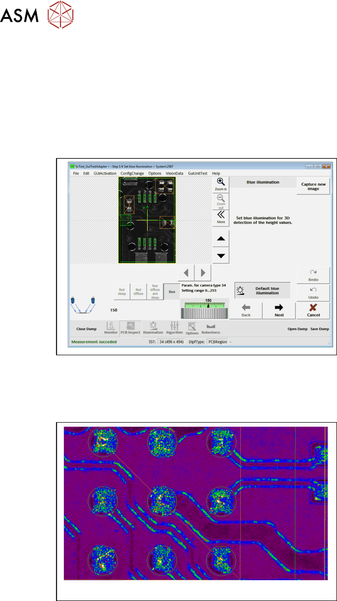
"Blue" lighting is preset for solder paste inspection, to ensure that the height profile image can be
calculated correctly. The solder deposits must appear bright enough. You can modify the lighting
intensity (setting range 0….255) under Param. for camera type. If the lighting is too dark, a hint
is displayed at the end of the Teaching wizard.
●
Areas with green border = component description
●
Areas with orange border = areas that are being teached (teaching area)
●
Areas with yellow border = inspection area
The illuminated solder deposits can be seen in details here:
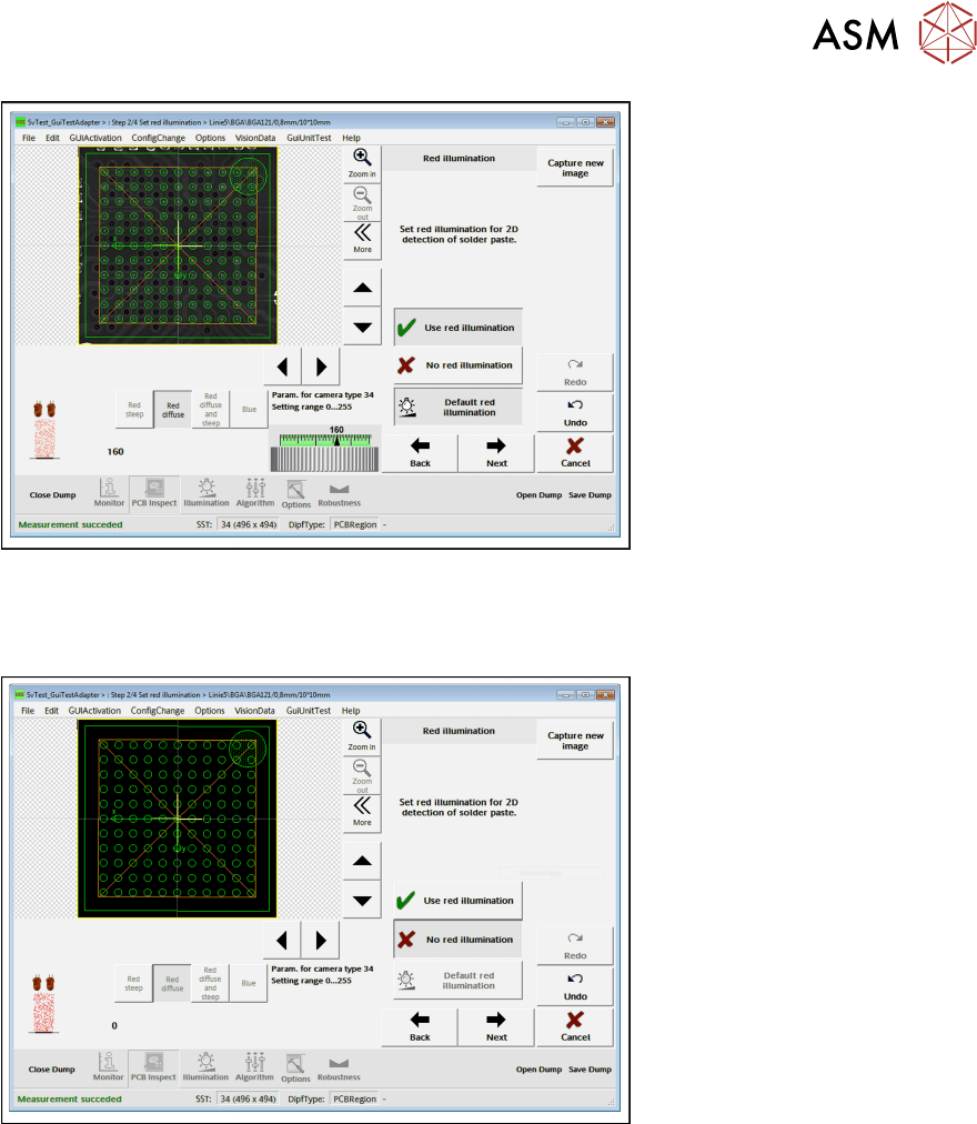
The red lighting is normally not needed and should not be used for runtime reasons. However, if
not all solder deposits are found during the teaching procedure (for example, because greater
areas of pads are not covered with solder paste), switch on the red light. The additional information
of images with red lighting improves the teaching.
► Click on the Next button.
Switching on the red lighting
If you use the red lighting, you should adjust the intensity under Param. for camera type in such a
way that free pad areas are displayed with a grey value of 255 (i.e. white).
4 Teaching Inspection Areas at the Station
4.2 Teaching Solder Paste Inspection (SPI)
User Manual / Bedienungsanleitung Onboard PCB Inspection 06/2018 51
► Select Use red illumination and click on Next.
Switching off the red lighting
► Select No red illumination to switch off the red lighting.
► Click on the Next button.