00198375-02_UM_OnBoardPCB-Inspection-R18-1_DE_EN.pdf - 第44页
2 What is Onboard PCB Inspection? 2.4 Prerequisites and Restrictions 44 User Manual / Bedienungsanleitung Onboard PCB Inspection 06/2018 Prerequisites for shields: ● There must be enough space between the components alre…
2 What is Onboard PCB Inspection?
2.4 Prerequisites and Restrictions
User Manual / Bedienungsanleitung Onboard PCB Inspection 06/2018 43
2.4.2 Regarding Solder Paste Inspection (SPI)
NOTICE
No complete substitute for SPI-AOI
The Solder Paste Inspection is not a complete substitute for SPI-AOI. It only produces a
good/bad result.
Restrictions
●
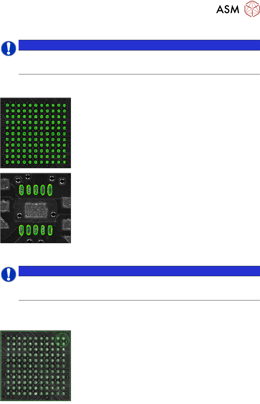
No offsets are recognized or only clear solder bridges are recognized.
Prerequisites for BGA:
●
The diameter of solder pads must be ≥ 0.15 mm.
Prerequisites for "non"BGAs:
●
The solder pads must have a pitch of ≥ 0.4mm.
2.4.3 Regarding Before Placement Inspection (BPI)
NOTICE
The offset inspection only permits a good/bad result.
The offset inspection only permits a good/bad result. This is not proof of placement accur-
acy.
General Requirements
●
The smaller the process variations during solder paste printing are, the less is the pseudo er-
ror rate. The pseudo error rate is higher in the case of greater process variations.
Prerequisites for BGA, LGA or QFP components:
●
Lost components are only recognized reliably up to a MINIMUM
size of 0201.
2 What is Onboard PCB Inspection?
2.4 Prerequisites and Restrictions
44 User Manual / Bedienungsanleitung Onboard PCB Inspection 06/2018
Prerequisites for shields:
●
There must be enough space between the components already
placed (general rule is approx. a space equal to the height of the
component around the components). Otherwise, there is the
danger of a reduced performance in the recognition of lost com-
ponents (both increased "false alarms" and "missed defects").
●
The permissible height of the components already placed is <
1mm.
●
Components which are only partly inside the inspection area are
NOT permitted.
●
Lost components are only recognized reliably up to a MINIMUM
size of 0201.
●
The permissible height of the components already placed is less
than 1 mm.
●
The smallest component size which can be inspected is the
0201.
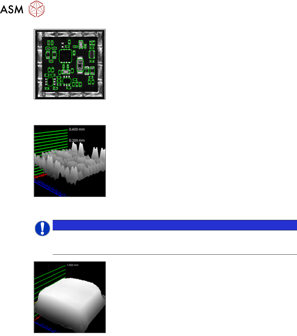
This image shows a height profile in which the height of all compon-
ents is significantly less than 1 mm.
2.4.4 Regarding After Placement Inspection (API)
NOTICE
The offset inspection only permits a good/bad result.
The offset inspection only permits a good/bad result. This is not proof of placement accur-
acy.
Prerequisites:
●
The permissible height of the components already placed is <
1mm.
●
The smallest component size which can be inspected is the
0201.
3 Programming and Download
3.1 Assigning Inspection Options to the Placement Position
User Manual / Bedienungsanleitung Onboard PCB Inspection 06/2018 45
3 Programming and Download
3.1 Assigning Inspection Options to the Placement Position
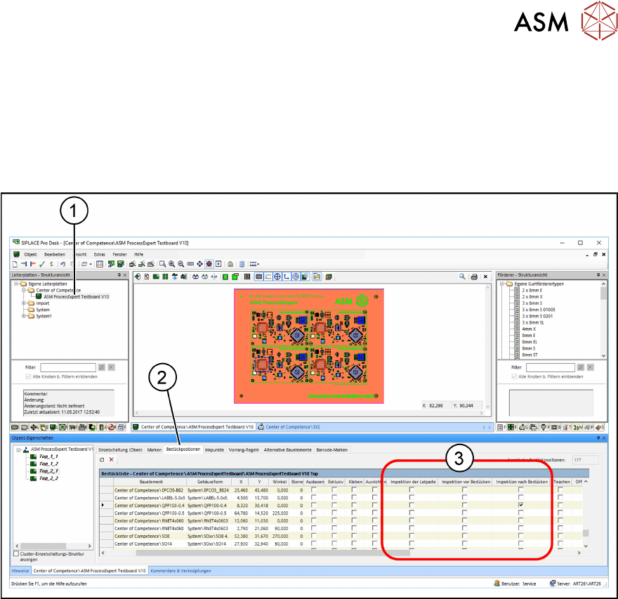
Enable the inspection options for the relevant placement position in the SIPLACE Pro Board Editor.
► Open the required board (1) in the SIPLACE Pro Board Editor.
► Select the Placements (2) tab.
► Enable the inspection options (3) for the relevant placement position.
●
Solder Paste Inspection
– The Solder Paste Inspection (SPI) is performed on areas of the board on which the quality
of the solder paste needs to be inspected. It is performed with the PCB camera of the first
machine in the line.
●
Before Placement Inspection
– Before Placement Inspection (BPI) is performed on areas of the board on which the poten-
tial absence of previously placed components or the presence of lost components needs to
be checked directly before placement.
●
After Placement Inspection
– After Placement Inspection (API) is performed on those board areas on which the pres-
ence of particular components (e.g. BGA, QFP, shield) needs to be inspected directly after
placement.
These three inspection options can be combined with one another as required.
3.2 Download to the Station
When the recipe data with the enabled inspection options are downloaded for the first time to the
station, you first need to teach the areas of the individual placement positions. Reference images of
the PCB areas to be inspected are acquired. These images are used to create the inspection
model. Take care during teaching to ensure an inspection as robust as possible. This reference
(target state) is then compared to the actual state of the placement positions to be inspected, dur-
ing the placement process. If both states match, placement will be performed. If they do not match,
placement will be stopped with a detailed error message and the operator will need to take action.