00198375-02_UM_OnBoardPCB-Inspection-R18-1_DE_EN.pdf - 第63页
5 Inspection Process at the Station 5.3 Handling of Bad Inspection Results User Manual / Bedienungsanleitung Onboard PCB Inspection 06/2018 63 5.3.2 Lost Components Recognized If lost components are detected, the relevan…
5 Inspection Process at the Station
5.2 Comparing Solder Height Differences From Model
62 User Manual / Bedienungsanleitung Onboard PCB Inspection 06/2018
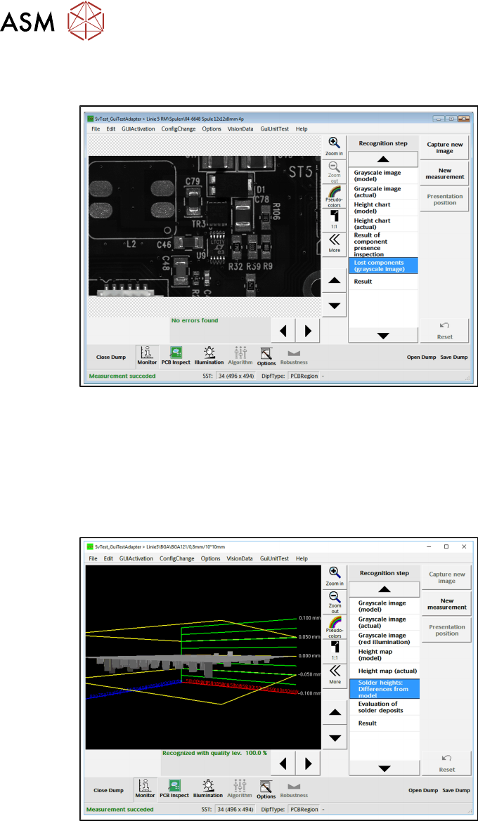
Good example for successful inspection of components after placement (no lost
components found)
Good example
5.2 Comparing Solder Height Differences From Model
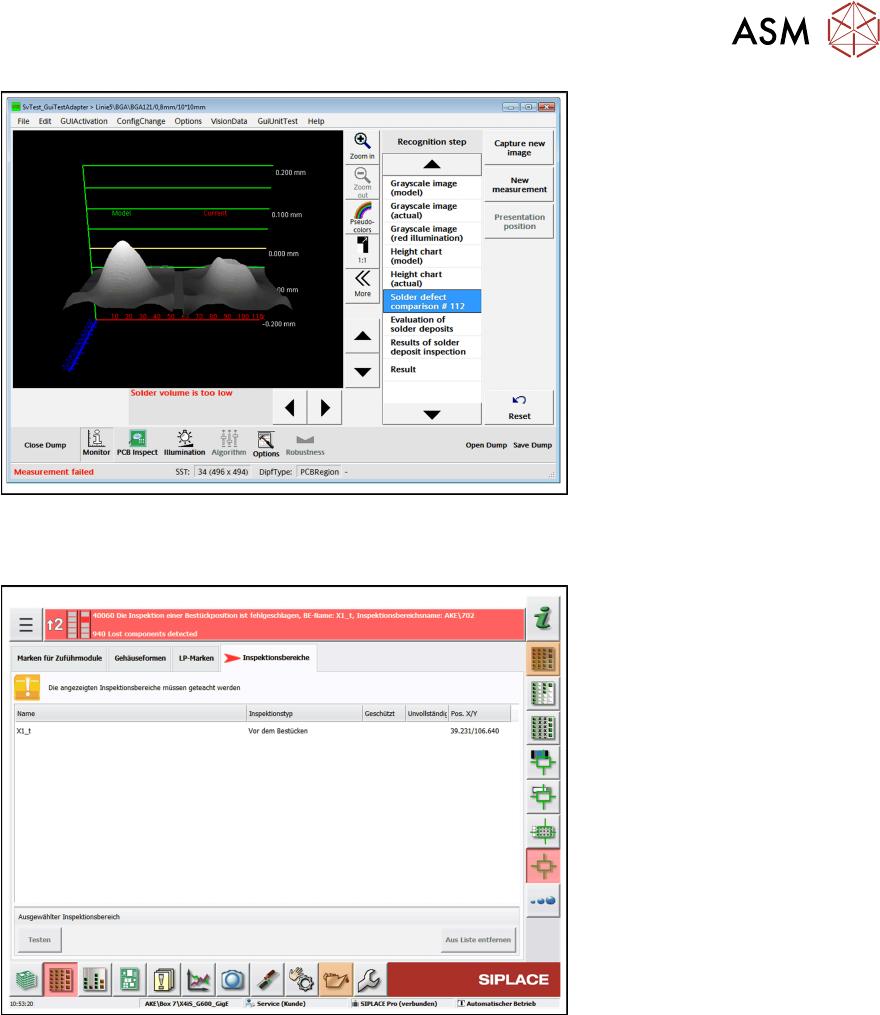
Here, a 3D view indicates for each solder deposit how strong its calculated average solder height
deviates from the reference value (model). The borders are shown as yellow rectangles at the cor-
responding Z position.
► Go to Recognition step and select Solder heights: differences from model.
5.3 Handling of Bad Inspection Results
5.3.1 Compare solder deposits
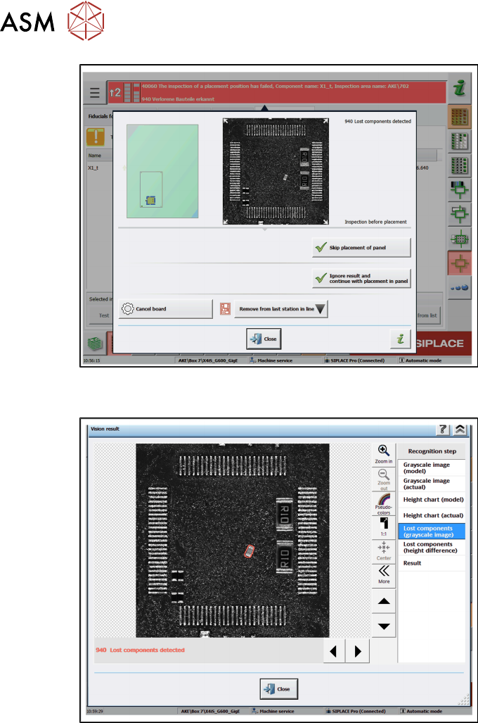
If errors occur, solder deposits can be compared. In the example, the reference image is compared
with the actual image of the solder pad. The diagram shows the difference and reports if the solder
volume is too low.
► Go to Recognition step and select Solder defect comparison# xxx.
5 Inspection Process at the Station
5.3 Handling of Bad Inspection Results
User Manual / Bedienungsanleitung Onboard PCB Inspection 06/2018 63
5.3.2 Lost Components Recognized
If lost components are detected, the relevant error message will be shown.
► Click on the error message to perform troubleshooting.
ð The following view will be shown.
5 Inspection Process at the Station
5.3 Handling of Bad Inspection Results
64 User Manual / Bedienungsanleitung Onboard PCB Inspection 06/2018
► Decide how you want to handle the error and perform one of the actions shown.
► Click on the image to open the following view. The relevant details will be shown.