00198375-02_UM_OnBoardPCB-Inspection-R18-1_DE_EN.pdf - 第60页
4 Teaching Inspection Areas at the Station 4.4 Teaching with After Placement Inspection 60 User Manual / Bedienungsanleitung Onboard PCB Inspection 06/2018 Tips and tricks ● During the teaching procedure and directly aft…
4 Teaching Inspection Areas at the Station
4.3 Teaching with Before Placement Inspection (BPI)
User Manual / Bedienungsanleitung Onboard PCB Inspection 06/2018 59
4.3.4 Applying the Successful Teaching Run
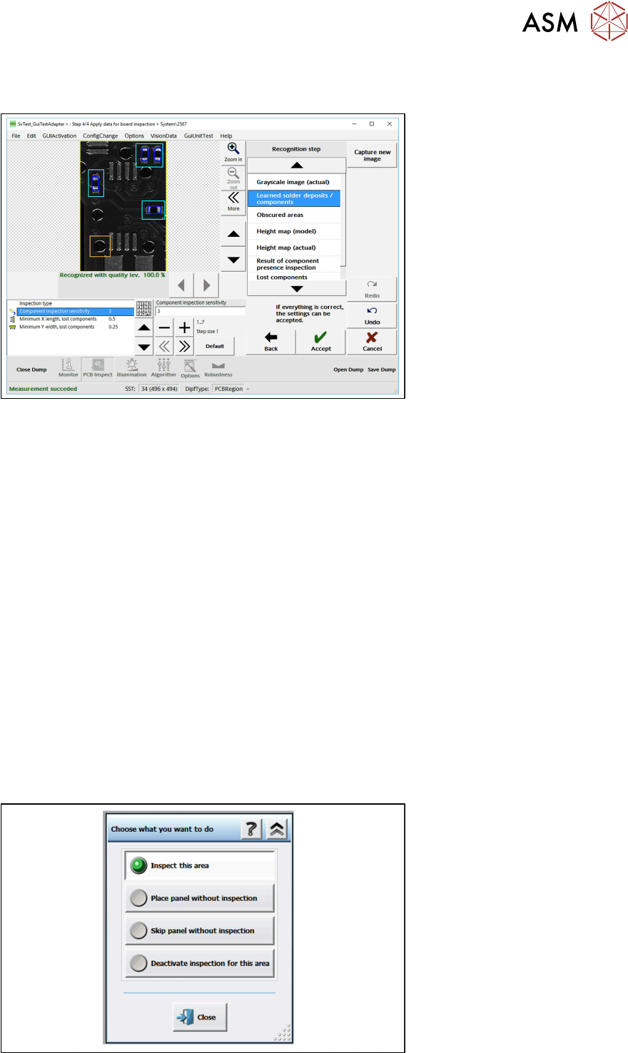
► Go to Recognition step and click on Learned solder deposits/components.
●
Components which have been taught have a blue border.
●
Teach areas have a turquoise border.
●
Exclusion areas have an orange border.
In the example you can see four detected components in the three defined teaching areas (marked
with a turquoise border). The hole in the board, found as an exclusion area, is marked with an or-
ange border.
Parameters
Various parameters can be set to improve the result.
●
Inspection type
– Shows the setting of the inspection type in SIPLACE Pro for your information.
●
Sensitivity of CO inspection
– Global value without a unit to set the sensitivity of the procedure. Especially for recognizing
lost components. Value range between 1 (max. sensitivity) and 7 (max. robust). If many
false alarms occur, increase this value.
●
Minimum X length of lost components and Minimum Y length of lost components
– Here, you can set the minimum size of components that are to be recognized as lost.
► If you are satisfied with the result, click on Accept to apply the teaching result and save it at
the station.
ð A dialog box will open in which you can select how to continue.
4 Teaching Inspection Areas at the Station
4.4 Teaching with After Placement Inspection
60 User Manual / Bedienungsanleitung Onboard PCB Inspection 06/2018
Tips and tricks
●
During the teaching procedure and directly afterwards, an inspection will be performed with
the model which has just been inspected. These results can also be selected in the Recogni-
tion step list and will be shown in the image view.
– Result of component presence inspection
– Lost components (grayscale image)
●
Only those components which were recognized during teaching will be checked for presence.
If a component to be checked is not marked with a blue border here, it was not found.
– If defects are already detected here, teach again with a better sample PCB.
– Select stronger lighting, correct the teaching areas and repeat the procedure.
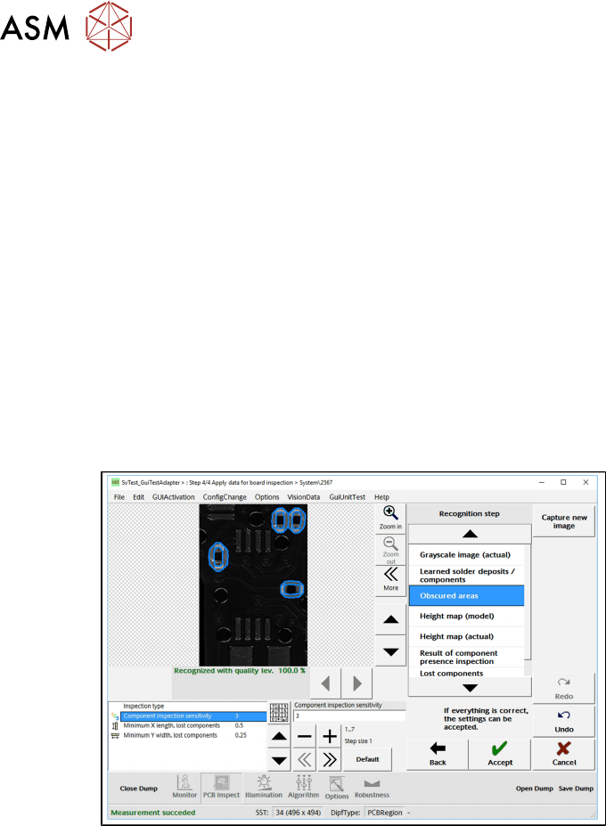
4.3.4.1 Checking Obscured Areas
Here, all areas that are obscured by a teached component are highlighted. If more components
that were not teached are located in these areas, these were not teached because they are ob-
scured.
► Go to Recognition step and select Obscured areas.
4.4 Teaching with After Placement Inspection
The teaching procedure for After Placement Inspection (API) is the same as that for Before Place-
ment Inspection (BPI).
Tips and tricks
●
When teaching with After Placement Inspection (API), we advise using only one teaching
area. The component which has just been placed should be fully covered by this area.
5 Inspection Process at the Station
5.1 Successful Inspection Results
User Manual / Bedienungsanleitung Onboard PCB Inspection 06/2018 61
5 Inspection Process at the Station
5.1 Successful Inspection Results
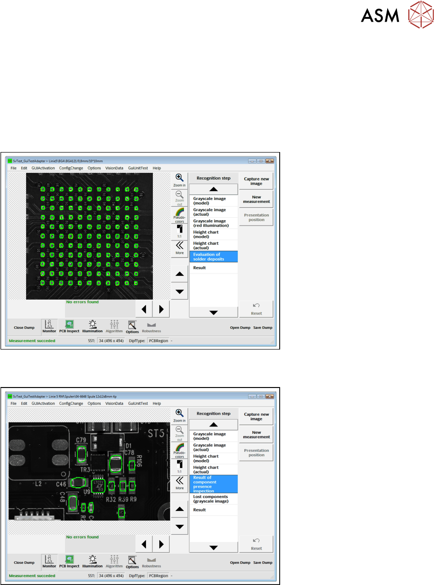
If the inspection was completed successfully, the relevant dialog will be shown. A few examples of
successful inspection results are shown below.
Good example for successful solder paste inspection
Good example for successful inspection of components before placement (required
components are present)