00198375-02_UM_OnBoardPCB-Inspection-R18-1_DE_EN.pdf - 第51页
4 Teaching Inspection Areas at the Station 4.2 Teaching Solder Paste Inspection (SPI) User Manual / Bedienungsanleitung Onboard PCB Inspection 06/2018 51 ► Select Use red illumination and click on Next . Switching off th…
4 Teaching Inspection Areas at the Station
4.2 Teaching Solder Paste Inspection (SPI)
50 User Manual / Bedienungsanleitung Onboard PCB Inspection 06/2018
4.2 Teaching Solder Paste Inspection (SPI)
You need to define the area with the solder deposits to be inspected.
4.2.1 Setting the Illumination.
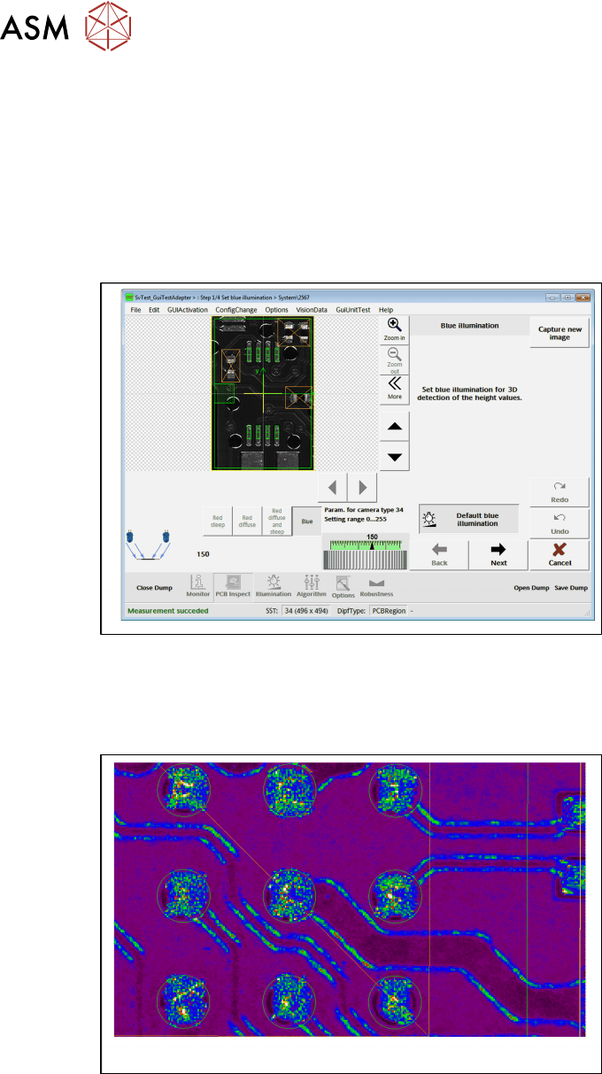
"Blue" lighting is preset for solder paste inspection, to ensure that the height profile image can be
calculated correctly. The solder deposits must appear bright enough. You can modify the lighting
intensity (setting range 0….255) under Param. for camera type. If the lighting is too dark, a hint
is displayed at the end of the Teaching wizard.
●
Areas with green border = component description
●
Areas with orange border = areas that are being teached (teaching area)
●
Areas with yellow border = inspection area
The illuminated solder deposits can be seen in details here:
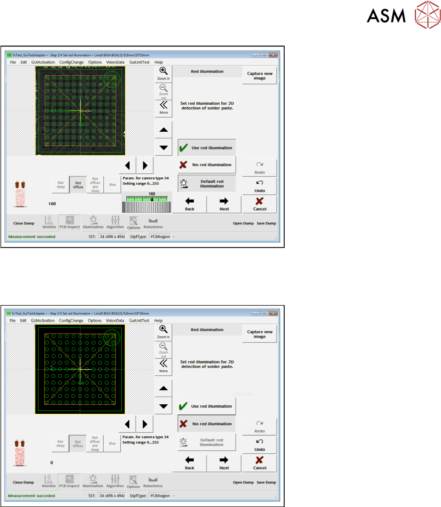
The red lighting is normally not needed and should not be used for runtime reasons. However, if
not all solder deposits are found during the teaching procedure (for example, because greater
areas of pads are not covered with solder paste), switch on the red light. The additional information
of images with red lighting improves the teaching.
► Click on the Next button.
Switching on the red lighting
If you use the red lighting, you should adjust the intensity under Param. for camera type in such a
way that free pad areas are displayed with a grey value of 255 (i.e. white).
4 Teaching Inspection Areas at the Station
4.2 Teaching Solder Paste Inspection (SPI)
User Manual / Bedienungsanleitung Onboard PCB Inspection 06/2018 51
► Select Use red illumination and click on Next.
Switching off the red lighting
► Select No red illumination to switch off the red lighting.
► Click on the Next button.
4 Teaching Inspection Areas at the Station
4.2 Teaching Solder Paste Inspection (SPI)
52 User Manual / Bedienungsanleitung Onboard PCB Inspection 06/2018
4.2.2 Inspecting the Solder Deposit Teaching Area
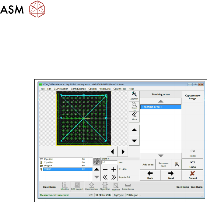
The area to be inspected and in which the solder deposits are located, needs to be defined. This
area must be defined for the teaching procedure. The solder deposits in this taught area will then
be inspected at the station.
As a default a teaching area has already been defined for each lead group in the component de-
scription. The example shows all the ball leads for a BGA.
As a rule, you will not need to add another teaching area. However, check the position and size of
the teaching area to make sure.
●
Area with green border = component description
●
Area with light blue border = the teaching area currently selected
The defined teaching areas can be selected at Teaching areas.
For further information please refer also to the Online Help.
Tips and tricks
●
The teaching area (light blue border) should be slightly bigger than the area with the solder
deposits actually is.
●
You may need to move the teaching area so that all the solder deposits can be reached.
●
Only define the solder deposit area as the teaching area. For example, four teaching areas for
QFPs (a separate teaching area per connection group).
●
When using larger QFPs, you may find that not all the solder deposits are completely visible
on the first teaching run.
– Solution: increase the teaching area accordingly and take another image.
► Click on the Next button.