CP7 training(6.0) (1).pdf - 第87页
FK-9F98-27 CP-7 Series T raining T ext for Service Engineers Edition 6.0 Chapter 5. Loader and Con veyor Adjustment [19/28] <I/O → S tandard → IN> Sensor Location X0A9 IN-CONVEYOR MID-ST OPPER UPPER LIMIT CHECK X0A…
FK-9F98-27 CP-7 Series Training Text for Service Engineers
Edition 6.0 Chapter 5. Loader and Conveyor Adjustment [18/28]
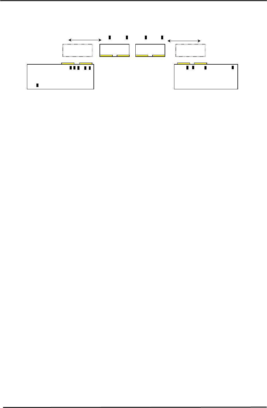
5.22 PCB Check Sensor Arrangement
IN Conveyor
IN Carrier OUT Carrier
OUT Conveyor
14
12
11
13
91078
6
5
23 4
1
PCB confirmation Sensors (Front view)
Figure 40
PCB Check Sensor location and function
1. Prevents boards that are longer than the M/C specification from being processed.
2. IN 2 Speed Reduction Check Sensor
2nd PCB speed reduction
3. IN 2 Arrival Check Sensor
2nd PCB IN Conveyor arrival check.
4. IN PCB Clearance Check Sensor
Checks the clearance between the 1st and 2nd PCB’s.
5. IN 1 Speed Reduction Check Sensor
1st PCB speed reduction
6. IN 1 Arrival Check Sensor
1st PCB IN Conveyor arrival check.
7. IN Carrier 2 Detection Check Sensor
Detects the 2nd PCB on the IN carrier when the IN carrier arrives at the forward end.
8. IN Carrier 1 Detection Check Sensor
Detects the 1st PCB on the IN carrier when the IN carrier arrives at the forward end.
9. OUT Carrier 2 Detection Check Sensor
Detects the 2nd PCB on the OUT carrier when the OUT carrier arrives at the forward end.
10. OUT Carrier 1 Detection Check Sensor
Detects the 1st PCB on the OUT carrier when the OUT carrier arrives at the forward end.
11. OUT 2 Arrival Check
Detects when the 2nd PCB arrives at the OUT conveyor.
12. OUT PCB Clearance Check Sensor
Checks the clearance between the 1st and 2nd PCB’s.
13. OUT 1 Arrival Check Sensor
Checks when the 1st PCB arrives at the OUT Conveyor.
14. Out Conveyor Arrival check Sensor
Checks for PCB’s on the out conveyor. (ready to move to next stage)
Fuji Machine Mfg. Co., Ltd. (Okazaki)
SMT Equipment Quality Assurance Dept.
CS Section
5-18
FK-9F98-27 CP-7 Series Training Text for Service Engineers
Edition 6.0 Chapter 5. Loader and Conveyor Adjustment [19/28]
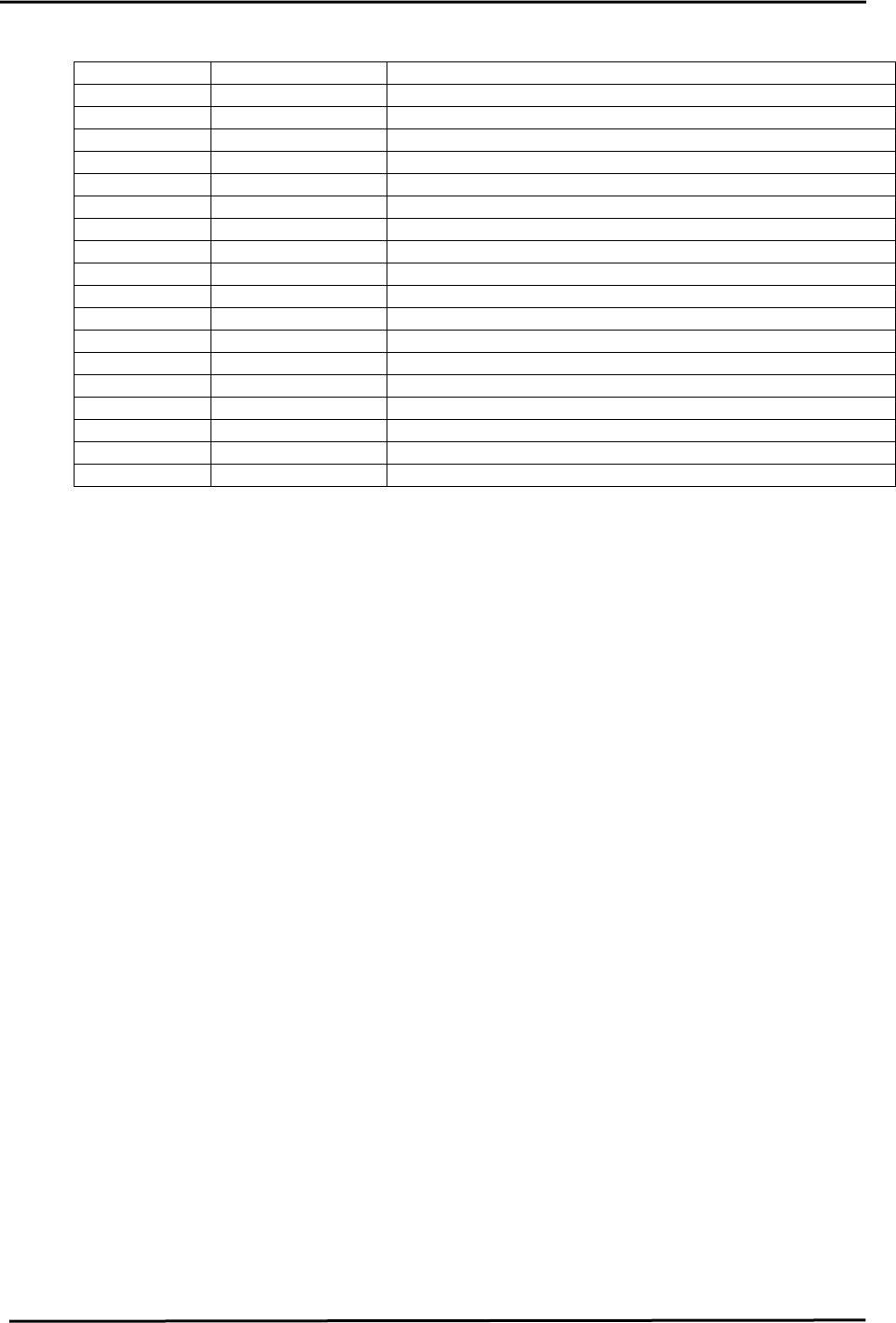
<I/O → Standard → IN>
Sensor Location
X0A9 IN-CONVEYOR MID-STOPPER UPPER LIMIT CHECK
X0AA IN-CONVEYOR MID-STOPPER LOWER LIMIT CHECK
X0AB (5) IN-CONVEYOR 1 SPEED DECELERATION POINT
X0AC (6) IN-CONVEYOR 1 PANEL ARRIVAL CHECK
X0AD (2) IN-CONVEYOR 2 SPEED DECELERATION POINT
X0AE (3) IN-CONVEYOR 2 PANEL ARRIVAL CHECK
X0AF (4) PANEL INTERVAL BETWEEN IN-CONVEYOR 1 AND 2
X0B0 (1) IN-CONVEYOR PANEL IN
X0B1 (8) IN-CARRIER FORWARD LIMIT PANEL CHECK (1)
X0B2 (7) IN-CARRIER FORWARD LIMIT PANEL CHECK (2)
X0C4 OUT-CONVEYOR MID-STOPPER UPPER LIMIT CHECK
X0C5 OUT-CONVEYOR MID-STOPPER LOWER LIMIT CHECK
X0C5 (13) OUT-CONVEYOR 1 PANEL ARRIVAL CHECK
X0C9 (11) OUT-CONVEYOR 2 PANEL ARRIVAL CHECK
X0CA (12) PANEL INTERVAL BETWEEN OUT-CONVEYOR 1and 2
X0CB (14) OUT-CONVEYOR UNLOADER PANEL ARRIVAL CHECK
X0CC (10) OUT-CARRIER FORWARD LIMIT PANEL CHECK (1)
X0CD (9) OUT-CARRIER FORWARD LIMIT PANEL CHECK (2)
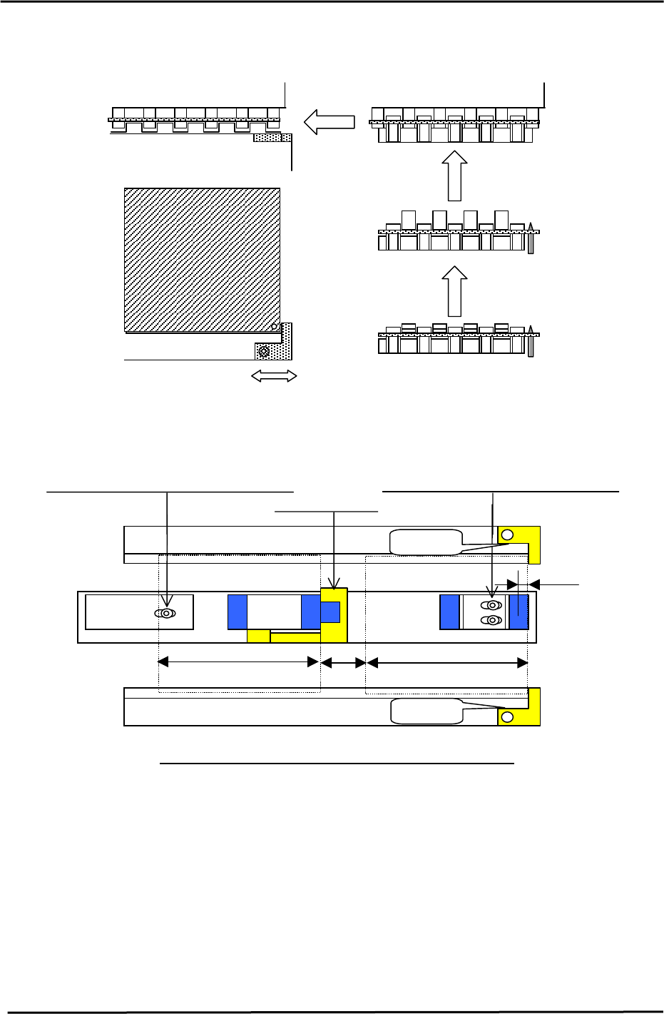
5.23 PCB Stopper and Check Sensor Adjustment
<<IN Conveyor (Fixed) Stopper Installation>>
Install the stoppers and adjust the sensors for 2-PCB-loading, using the maximum length
board: (CP-732/733E: 170MM) (CP-742/743(M)E: 220MM)
Install the stoppers only after the X, Y, and Z, axes, “Loading Position” has been calibrated.
1. With the first PCB stoppers from the In conveyor removed, move the XY table to the IN loading
position. (DO NOT raise the Z-axis) The 1
st
PCB moveable stopper should be down. (Turn
On “Y079” to lower the 1
st
PCB stopper)
2. Turn ON “Y044”, (Main clamp open), and position the maximum length board (for 2 PCB’s) on
the reference and secondary pins. Turn ON “Y043” (Main clamp close), and clamp the PCB.
3. Turn ON “Y072”, (In carrier close) , “Y074”, (In carrier advance) ,and “Y073”, (In carrier open).
Manually raise the Z to the IN loading position.
4. Turn ON “Y072” (In carrier close), and “Y044”(Main clamp open), and lower Z to the “Z0”
position. (The PCB should now be clamped on the carrier.)
5. Turn ON “Y075”(In carrier retract), “Y076” (In lifter up), and “Y073” (In carrier open), “Y077” (In
lifter down), “Y072” (In carrier close), and “Y074” (In carrier advance). (the PCB is now loaded
at the correct position on the IN conveyor.) See Fig. 41.
6. Set the first PCB stoppers against the leading edge of the PCB. (be careful not to move the
board)
7. Loosen the sensor positioning bolt for the first PCB check sensor and position the sensor 5mm
from the leading edge of the first PCB. See Fig. 42.
Fuji Machine Mfg. Co., Ltd. (Okazaki)
SMT Equipment Quality Assurance Dept.
CS Section
5-19
FK-9F98-27 CP-7 Series Training Text for Service Engineers
Edition 6.0 Chapter 5. Loader and Conveyor Adjustment [20/28]
8. Set the IN PCB clearance check sensor switch to “D_ON”, and both the arrival and speed
reduction sensor switches to “L_ON”.
Figure 41
1
st
PCB Stopper
5mm
15mm
170mm (220mm)
nd
No Gap
2
n
d
PCB Stopper
170mm (220mm)
st
1
st
PCB Stopper
Sensor positioning bolt for the 1
st
PCB
Sensor positioning bolt for the 2
nd
PCB
No Gap
Stopper and Sensor Positioning for the IN conveyor.
Figure 42
Fuji Machine Mfg. Co., Ltd. (Okazaki)
SMT Equipment Quality Assurance Dept.
CS Section
5-20