CP7 training(6.0) (1).pdf - 第89页
FK-9F98-27 CP-7 Series T raining T ext for Service Engineers Edition 6.0 Chapter 5. Loader and Con veyor Adjustment [21/28] <<IN Carrier Sensor Adjustment>> 1. Load two PCBs on the IN carrier . “X0B1” (In ca …
FK-9F98-27 CP-7 Series Training Text for Service Engineers
Edition 6.0 Chapter 5. Loader and Conveyor Adjustment [20/28]
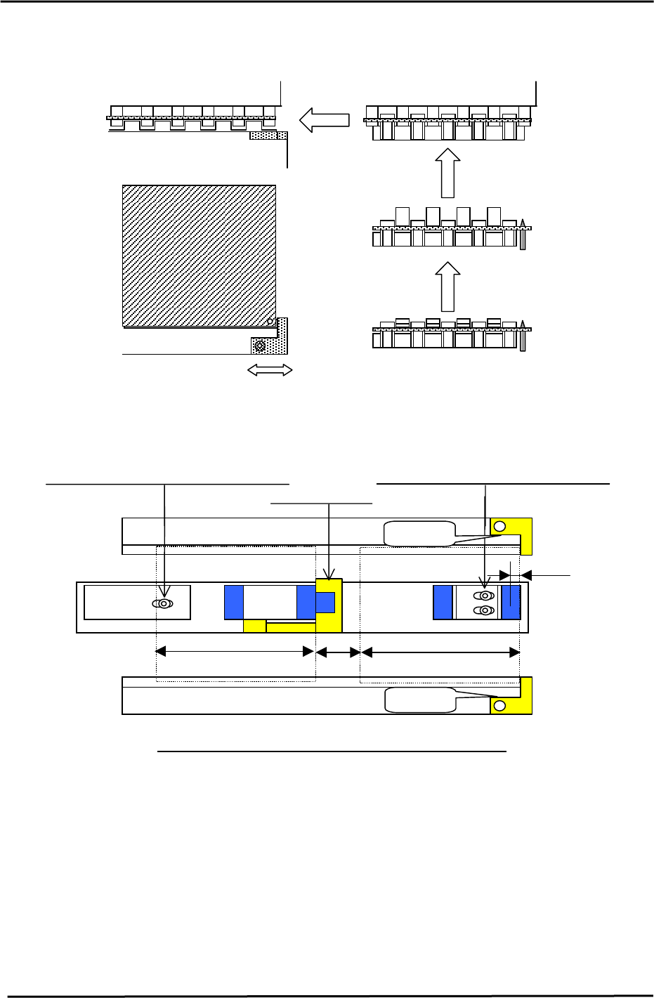
8. Set the IN PCB clearance check sensor switch to “D_ON”, and both the arrival and speed
reduction sensor switches to “L_ON”.
Figure 41
1
st
PCB Stopper
5mm
15mm
170mm (220mm)
nd
No Gap
2
n
d
PCB Stopper
170mm (220mm)
st
1
st
PCB Stopper
Sensor positioning bolt for the 1
st
PCB
Sensor positioning bolt for the 2
nd
PCB
No Gap
Stopper and Sensor Positioning for the IN conveyor.
Figure 42
Fuji Machine Mfg. Co., Ltd. (Okazaki)
SMT Equipment Quality Assurance Dept.
CS Section
5-20
FK-9F98-27 CP-7 Series Training Text for Service Engineers
Edition 6.0 Chapter 5. Loader and Conveyor Adjustment [21/28]
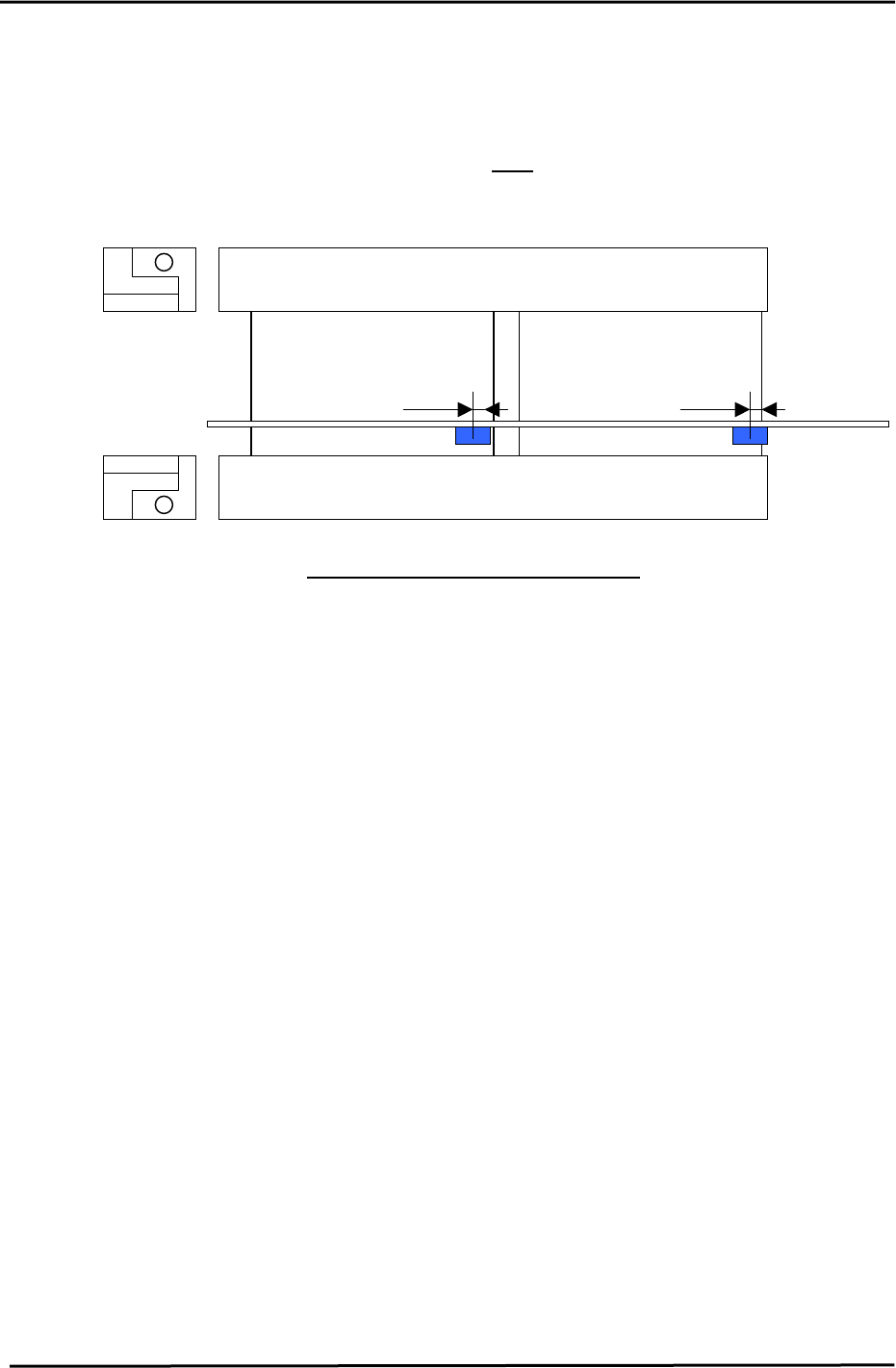
<<IN Carrier Sensor Adjustment>>
1. Load two PCBs on the IN carrier. “X0B1” (In carrier 1 detection check), “X0B2” (IN carrier 2
detection check) shall come ON when “Y074”, (In carrier advance) is ON. Adjust the sensor
position 5mm from the leading edge of each board. Ensure that the sensor switch is set to
“L_ON”. And make sure that the volume is at
MAX position.
(1
st
PCB)
5mm
(2
nd
PCB)
5mm
Figure 43
IN Carrier
Sensor Positioning for the IN Carrier
Fuji Machine Mfg. Co., Ltd. (Okazaki)
SMT Equipment Quality Assurance Dept.
CS Section
5-21
FK-9F98-27 CP-7 Series Training Text for Service Engineers
Edition 6.0 Chapter 5. Loader and Conveyor Adjustment [22/28]
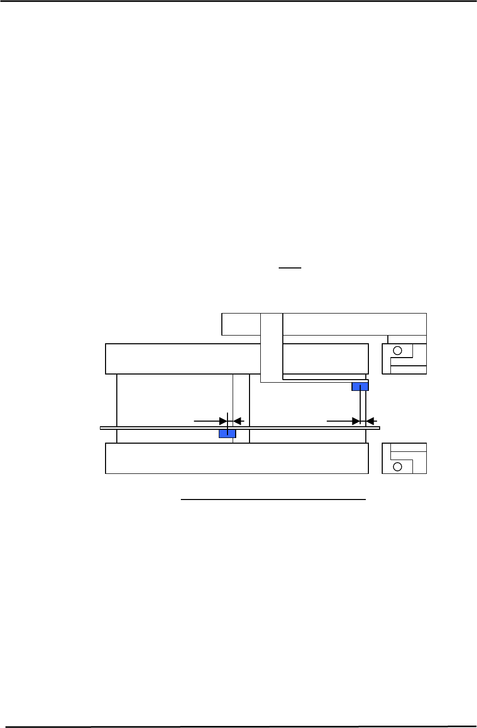
<<OUT Carrier Sensor Adjustment>>
Adjust the sensors for the OUT carrier as follows:
1. Load 2 PCBs on the IN carrier. Advance the carrier to the forward end position. (Continued from
the IN carrier adjustment.). Move the XY table to the IN loading position. (Do NOT raise the Z-
axis.)
2. Turn ON I/O, “Y044” (Main clamp open). Raise Z to the IN loading position.
3. Turn ON “Y043” (Main clamp close) and “Y073”,(IN carrier open). Lower the Z-axis to the “Z0”
position to load 2 PCBs onto the XY table. Then, move the main table to the unloading position.
4. Turn ON “Y082” (Out carrier close), “Y084” (Out carrier advance), and “Y083”(Out carrier open)
and raise the Z-axis raise to the ZL out position.
5. Turn ON “Y082”(Out carrier close) and “Y082” (Main clamp open). Lower Z to set to the same
condition as when the 2 PCBs were loaded on the IN carrier.
6. Adjust the sensor position so that “X0CC” (Out carrier 1 detection check), and “X0CD” (Out
carrier 2 detection check) are set 5mm from the leading edge of each Pcb. Set the sensor switch
to “L_ON”. And make sure that the volume is at
MAX position.
(1
st
PCB)
5mm
(2
nd
PCB)
5mm
OUT Carrier
Sensor Positioning for the Out Carrier
Figure 44
Fuji Machine Mfg. Co., Ltd. (Okazaki)
SMT Equipment Quality Assurance Dept.
CS Section
5-22