3OM-1343-008_w.pdf - 第116页
3-31 AKFEDT -ID (2) Material for Marks Copper Leaf Nickel Plating Solder Plating Solder Leveler Gold Plating Note (a) A copper leaf, a resist, a coating, a silk print, and a punched hole should not exist in the range of …
3-30
AKFEDT-ID
Table 3C2-2
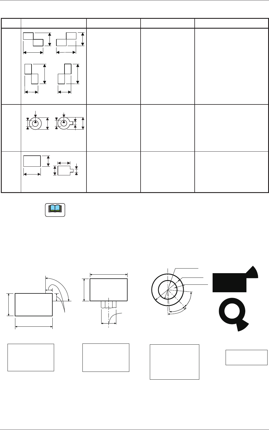
Mark Type D1 [mm] D2 [mm] Remarks
Checker (Rectangle)
D1
D1
D1
D1
D2
D2
D2
D2
or
or
(Front Side of Machine)
0.5 to 3.0 0.5 to 3.0
·
Mark Reference:
Contact of Two
Rectangles
Through Hole
(Round)
D2
D1
W
(Front Side of Machine)
D2
W
D1
Note: b
0.5 to 3.0 0.5 to 1.5
·
Mark Reference:
Center
·
D2: Size of a
punched hole
·
W: Min. 0.25 mm
Pad Mark
(Rectangle)
(Front Side of Machine)
D2
D1
D2
D1 Note: b
0.5 to 3.0 0.5 to 2.0
·
Mark Reference:
Center of Gravity
Note
(a) The error in the mark size should be within ±10%, compared with the
reference pattern.
(b) A through hole or a pad mark should have only one land which is
directed in increments of 45°.
(c) SpecicationsofLineextendedfromaPadMarkoraThroughHole.
Unit: mm
Range of Tangent
Lines related between
Pad Mark and Land
Range of Land
Location in
Increments of 45o
for Pad Mark
Range of Land
Location in
Increments of 90o
for Pad Mark
(Front Side of Machine)
1/3 of Side
0.5 to 2.0
0.5 to 2.0
Examples of
Land Locations
Range of Land
Location for
Through Hole
(45oat the bottom
right of the hole)
0.5 to 1.5
1.0 to 2.0
Min.0.25
45o
40o
40o
0.5 to 2.0
0.5 to 2.0
(Front Side of Machine)
(Front Side of Machine)
(Front Side of Machine)
Range of Tangent
Lines related between
Pad Mark and Land
1/3 of Side
(Range of Tangent
Lines related between
Pad Mark and Land)
Fig. 3C24
0711-003
1.2 Operation Data
3-31
AKFEDT-ID
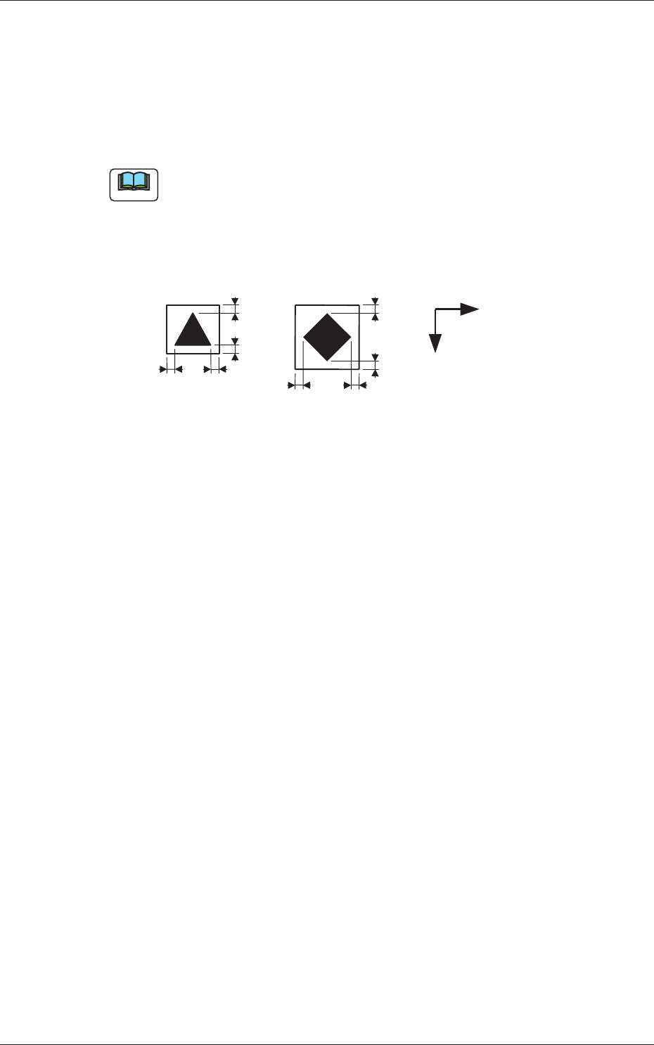
(2) Material for Marks
Copper Leaf
Nickel Plating
Solder Plating
Solder Leveler
Gold Plating
Note
(a) A copper leaf, a resist, a coating, a silk print, and a punched hole
should not exist in the range of 1.0 mm in both X and Y directions
from the outermost edges of a fi ducial mark. They may cause false
recognition.
Example:
1.0
1.0
1.0
1.0
1.0
1.0
1.0
1.0
Y
X
(Front Side of Machine)
Unit: mm
Fig. 3C25
(b) The shape of PCB (a cutout, a punched hole), the external elements
(light refl ected from a structure, light emitted from an external device,
etc.) may sometimes interfere with recognition of fi ducial marks.
(c) A fi ducial mark should make ample contrast with the surroundings.
(To prevent false recognition)
(d) Anything resembling a pattern similar to a fi ducial mark should not
exist in the designated recognition window. If one exists, it may cause
false recognition.
(e) A test may be required when the fi ducial mark cannot be recognized
because of the extreme warpage of the PCB.
0601-002
1.2 Operation Data

3-32
AKFEDT-ID
1.2.5 (A04) Setup Data
Note
Unless "Enable" is selected for a device to be set up, the machine does not
perform any setup operation on the device.
(A04_01)
Conveyor
"Enable" or "Disable" can be selected to determine whether the
conveyor width should be set up or not after a program change
operation.
Disable :
The conveyor width setup operation is not performed.
Enable :
The conveyor width setup operation is performed.
(A04_02)
PCB Y Position Arrangement
It can be determined whether or not the PCB transfer section should
be moved in the optimum Y direction according to the pattern program
when a program change operation is performed.
Mode
Select either "Enable" or "Disable" in the "Mode" text box of the label
"PCB Y Position Arrangement".
Disable :
The Y position of the PCB is not arranged.
Enable :
The Y position of the PCB is arranged.
Specify Method
When "Enable" is set in the "Mode" text box, select one of the
following options.
Specifi ed Position :
The conveyor Y position in the PCB
positioning section is moved to the
specifi ed position.
Base Conveyor Fixation :
The PCB positioning section is fi xed to
the reference position.
Position [mm]
When "Specifi ed Position" is set in the "Specify Method" text box,
specify the distance of the PCB Y position (center) to be shifted from
the machine’s positioning center.
0604-003
1.2 Operation Data