KY8030 Programmers Manual.pdf - 第53页
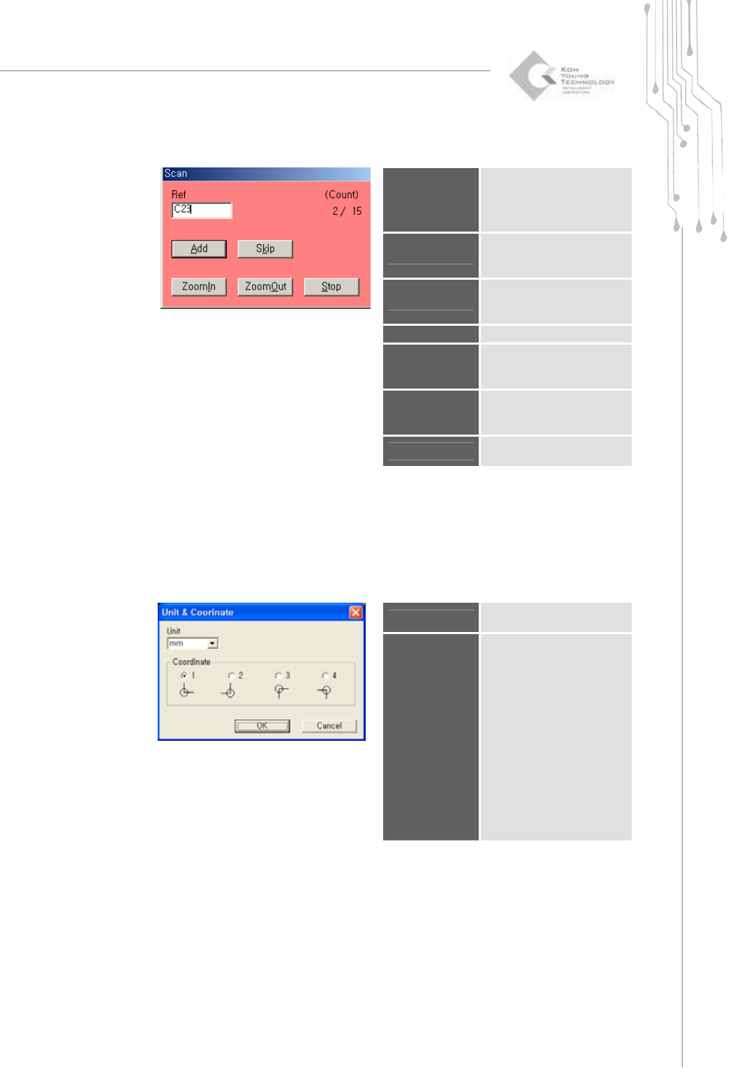
Program mers Manual | 5 1 The "Scan" Dialog Box Ref Part reference code. ※ Note: You may not us e the same part reference number twice. (Count) The number of pads found / The total number of pads scanned Add …
50 | KY-8030 Series(KYOS-2007001_rev0)
3DIn‐lineSolderPasteInspectionSystems
12) Scan Reference (Currently not used)
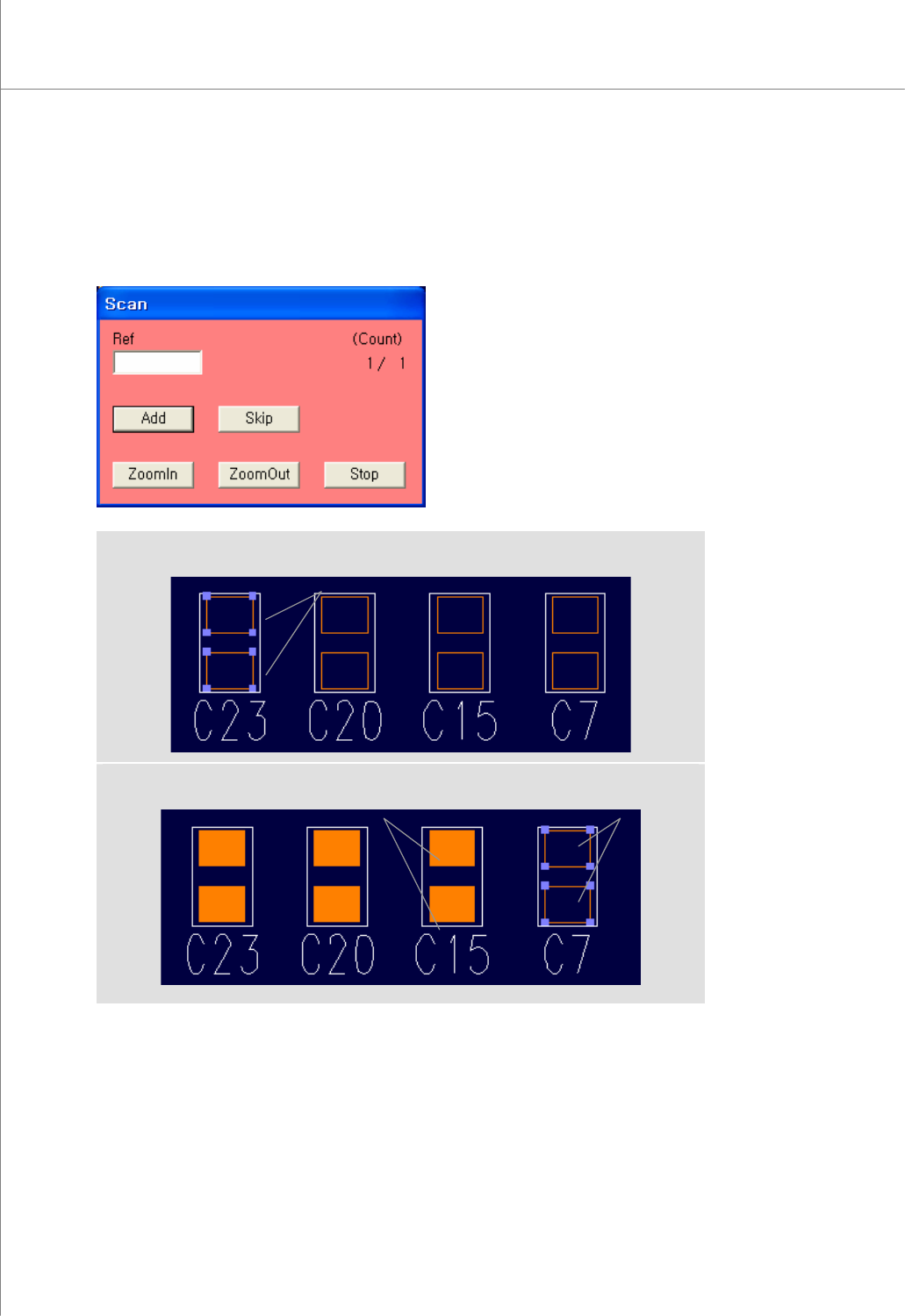
You can scan through a group of identical pads within a work area as if they were a
single part.
Open the "Scan" dialog box to enter a reference code.
(Selecting a Pad)
(After Performing "Scan Reference")
Selected pads automatically Referenced pads
Selected pads
Programmers Manual
| 51
The "Scan" Dialog Box
Ref
Part reference code.
※ Note: You may not use
the same part reference
number twice.
(Count)
The number of pads found /
The total number of pads
scanned
Add
Assign a part reference
code to a group of selected
pads.
Skip
Move to the next pad group.
Zoom In
Zoom in the screen based
on the current center
position.
Zoom Out
Zoom out the screen based
on the current center
position.
Stop
Stop scanning and close the
dialog box.
13) Unit & Coordinate
Open the "Unit & Coordinate" dialog box to specify a display unit and coordinate
system.
The "Unit & Coordinate" Dialog Box
Unit
Select a unit. (Available
units: mm, inches)
Coordinate
1: Lower Left
2: Lower Right
3: Upper Left
4: Upper Right
Select a coordinate system.
Increase X-values to the
right. / Increase Y-values
upward.
Increase X-values to the left.
/ Increase Y-values upward.
Increase X-values to the
right. / Increase Y-values
downward.
Increase X-values to the left.
/ Increase Y-values
downward.
52 | KY-8030 Series(KYOS-2007001_rev0)
3DIn‐lineSolderPasteInspectionSystems
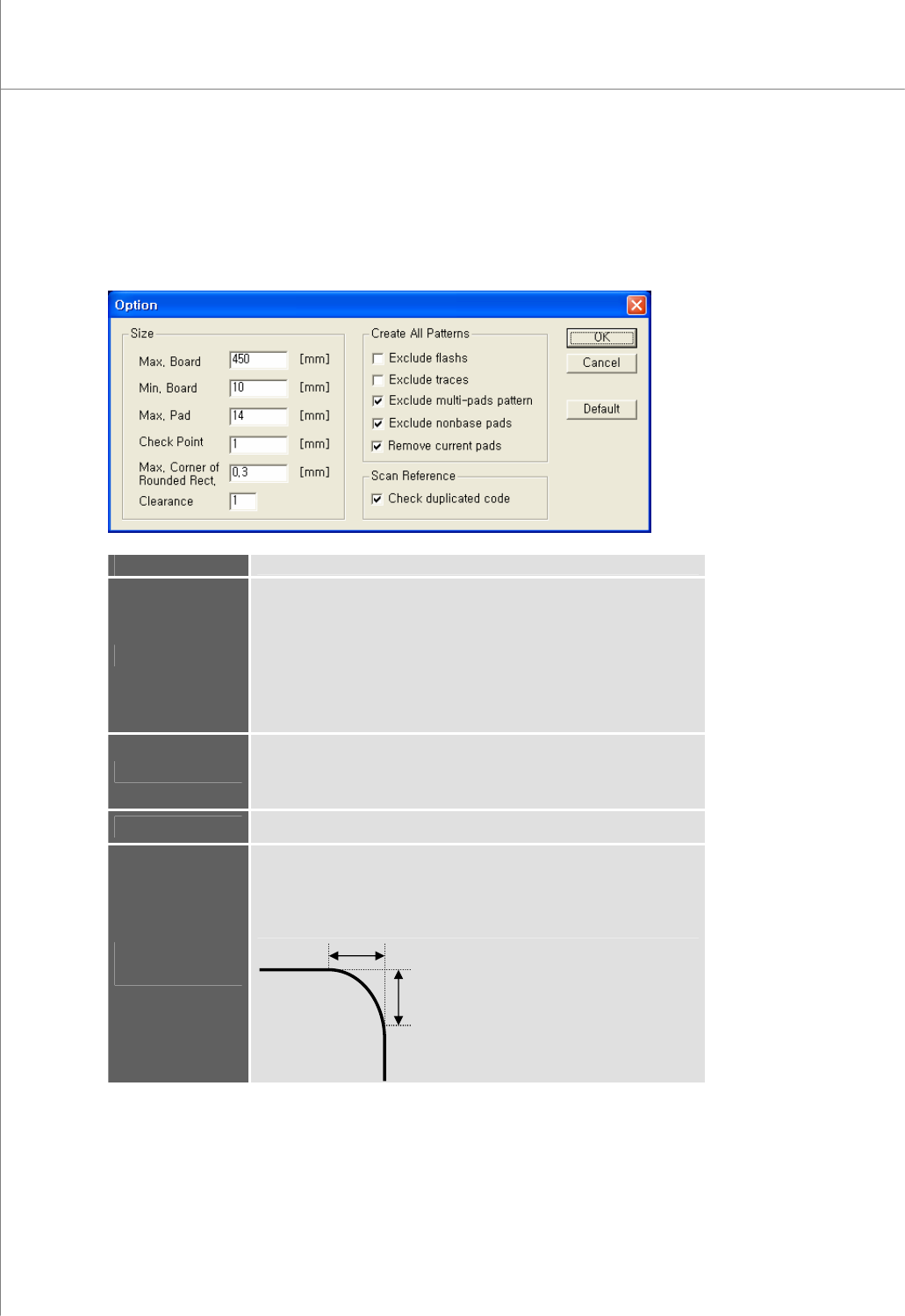
14) Option
Open the "Option" dialog box to specify option settings.
The "Option" Dialog Box["flashs" in box below should read "flashes"]
Max. Board
The maximum length of a PCB
Min. Board
The minimum length of a PCB.
When loading a Gerber file that contains a board with a
maximum/minimum size, make sure that the Gerber parameters are
valid.
※ Caution: If Gerber parameters are not set correctly, it may lead to
incorrect board size or position data, inhibiting normal PCB operation.
When opening a Gerber file in the RS274D format, make sure that the
Gerber parameters entered match the actual size of the PCB.
Max. Pad
The maximum length of a pad.
When performing "Create All Patterns", patterns are retrieved only
when the size of patterns is equal to or less than the Max Pad value.
Check Point
The size of a check point displayed on the screen
Max. Corner of
Rounded Rect.
The maximum offset value for a rounded rectangle.
This value differentiates rectangles and rounded rectangles from other
pattern shapes.
Offset
Offset