KY8030 Programmers Manual.pdf - 第77页
Programmers Manual | 75 6) Type the proper board size and the thickness of the stencil mask. Click Apply then the selected file will be opened. 7) Select in ord er to s et the fi ducia l. 8) Select pads which you wan t t…
74 | KY-8030 Series(KYOS-2007001_rev0)
3DIn‐lineSolderPasteInspectionSystems
⑤ Click the SetÆbutton to set all component attributes for an array-type PCB to the current values.
2.2. Usage Example (Creating a Job File)
Basic procedure is like followings.
- Load Pad File.
- Input the thickness of the stencil mask.
- Set the Fiducials.
- Set the inspection condition for the pads.
- Import CAD file or Pin CAD file(When available).
- Save Job file. (*.mdb)
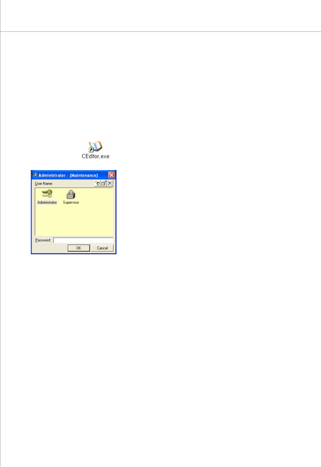
1) Double-click the
icon. A window will appear allowing you to select a
user account.
2) Select the desired user account, enter a password and click the OK button.
The CEditor program will be launched.
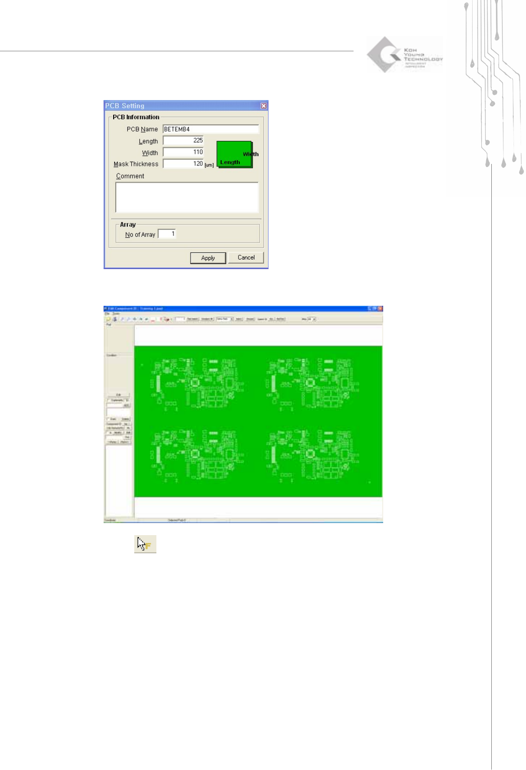
3) Click "File ▶ Load Pad file “ in the menu bar. The file selection window will appear.
4) Select a pad file (*.pad) and click the Open button. The selected file will be opened.
5) The following PCB setting window pops up.
Programmers Manual
| 75
6) Type the proper board size and the thickness of the stencil mask. Click Apply then
the selected file will be opened.
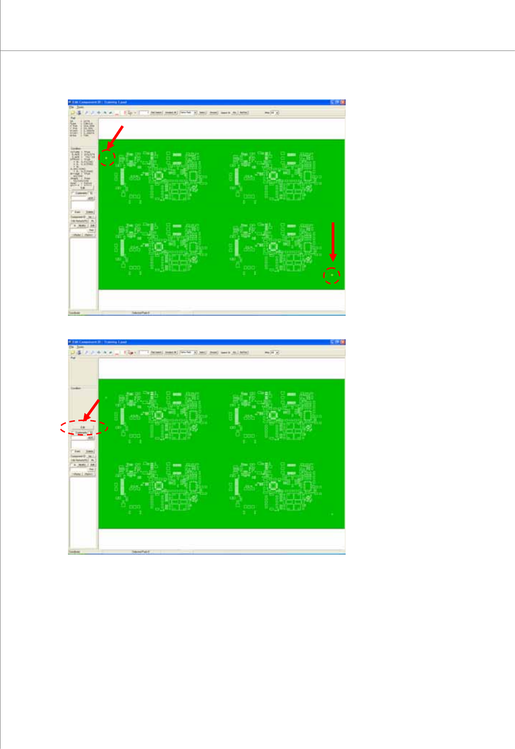
7) Select
in order to set the fiducial.
8) Select pads which you want to set as fiducial. (The color will be changed to the
yellow.)
76 | KY-8030 Series(KYOS-2007001_rev0)
3DIn‐lineSolderPasteInspectionSystems
9) Select arbitrary pad and click Edit button.
10) Change PAD Inspection Condition dialog box pops up.