KY8030 Programmers Manual.pdf - 第85页
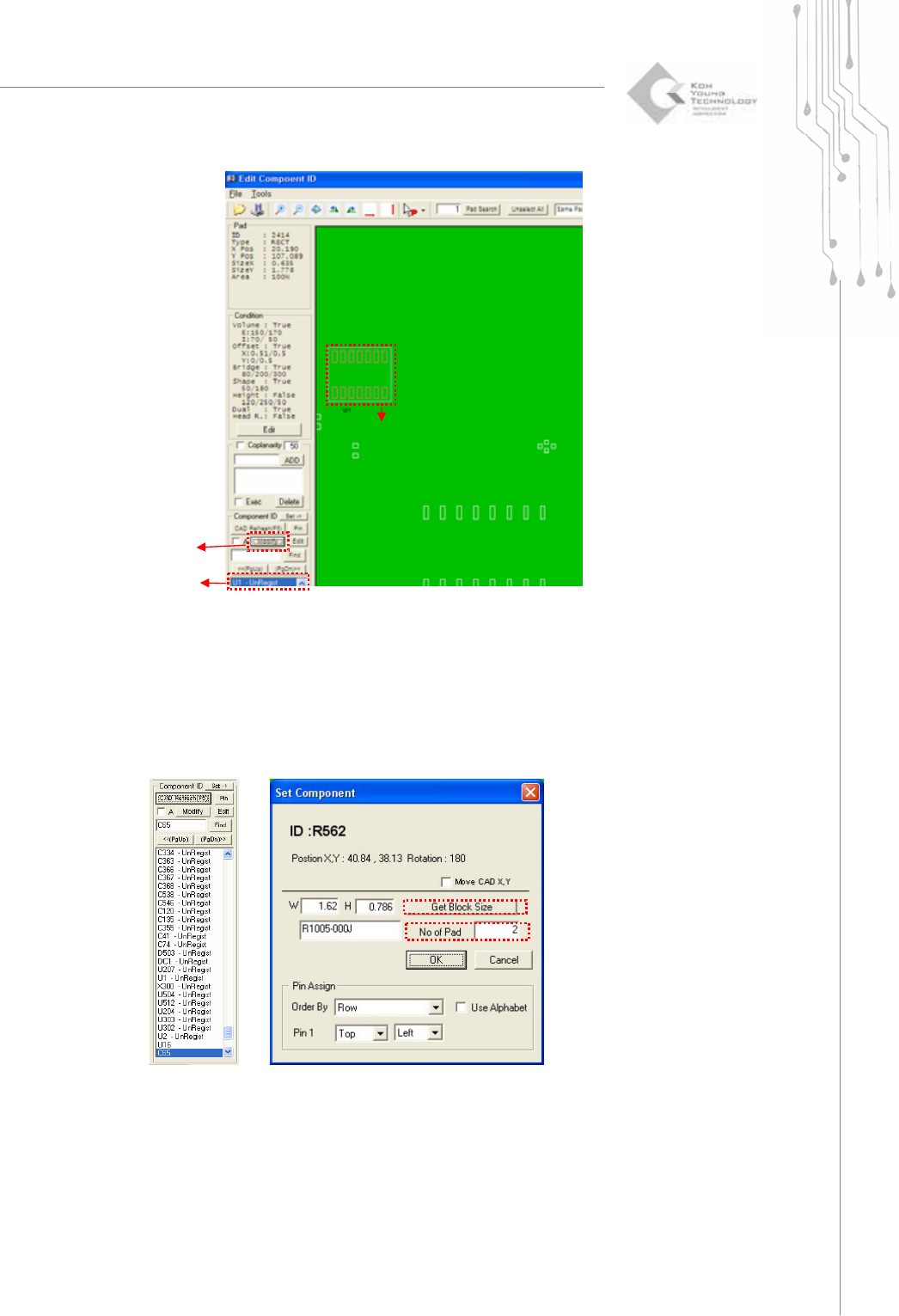
Programmers Manual | 83 2) Choose a not-matched component or component to be modified under the “C ompon ent ID ”. 3) Draw a box for that compone nt ID in PCB display. 4) Click the Modify button. The “Set Co mponent” win…
82 | KY-8030 Series(KYOS-2007001_rev0)
3DIn‐lineSolderPasteInspectionSystems
4) Click the Set button. The duplicated CAD file data will be displayed.
5) Click the CAD Refresh button or press the F5 key in the keyboard to display all
component and pin numbers.
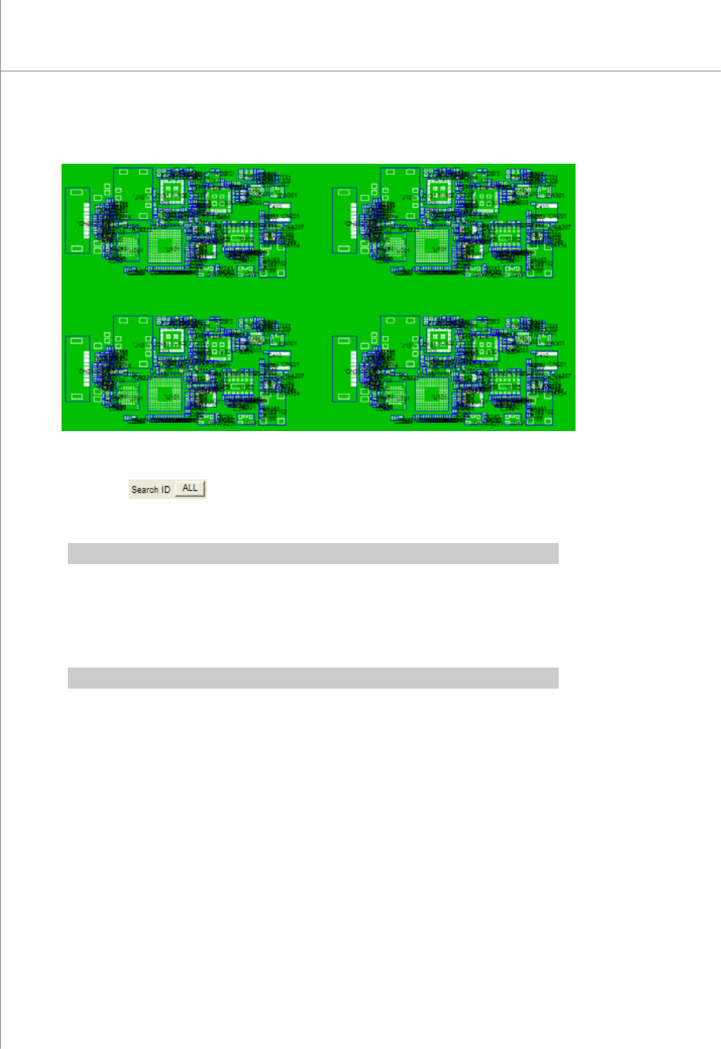
6) Click the
button under the “Search ID”. Assign a pin number to the
matched pin CAD and pad data and register it. Save the registered pin number in a
job file.
※ Note: Click the Not Find button under the "Search ID" to display unmatched data.
7) Component ID for 2,3 and 4 array will be properly registered.
8) Click the Save button to save the job data in a job file.
2.2.3. Modifying a Component ID
※ Note: Not applicable when pin CAD file is used..
1) Follow steps 1) - 11) in the previous example under 5.2.1.
Programmers Manual
| 83
2) Choose a not-matched component or component to be modified under the
“Component ID”.
3) Draw a box for that component ID in PCB display.
4) Click the Modify button.
The “Set Component” window will appear. Click OK.
②
①
③

84 | KY-8030 Series(KYOS-2007001_rev0)
3DIn‐lineSolderPasteInspectionSystems
Get Block Size : Recalculate the block size when the block was not correct.
No of Pad : Put the correct number of Pads for the components.
5) Modify component data as desired and click the OK button.
Once the component ID is registered, the "No match" sign for the modified
component will disappear.
6) Click the
button under the “Search ID”. Assign a pin number to the
matched pin CAD and pad data and register it. Save the registered pin number in a
job file.
7) Click the CAD Refresh button or press the F5 key in the keyboard to display all
component and pin numbers.
8) Click the Save button to save job data in a job file.