SMW200A_specs_en_3606-8037-22_v2700.pdf - 第50页
Version 27.00, October 2024 50 Rohde & Schwar z R&S ® SMW200A Vec tor Signal Generator Wideband baseband chara cteristics Internal baseband characteristic s (R&S ® SMW -B13XT optio n) The R&S ® SMW-B13XT …

Version 27.00, October 2024
Rohde & Schwarz R&S
®
SMW200A Vector Signal Generator 49
Standard baseband generator (R&S
®
SMW-B10 option) –
real-time operation (custom digital modulation)
See Digital Standards for Signal Generators specifications (PD 5213.9434.22).

Version 27.00, October 2024
50 Rohde & Schwarz R&S
®
SMW200A Vector Signal Generator
Wideband baseband characteristics
Internal baseband characteristics (R&S
®
SMW-B13XT option)
The R&S
®
SMW-B13XT provides I/Q paths that can be routed to the installed RF paths or to the analog I/Q outputs. Up to two signals
can be output at the same time, for example:
• Signal A is routed to RF path A, signal B to RF path B
• Signal A is routed to RF path A, signal B to analog I/Q out 1
D/A converter
Data rate
2400 MHz
Resolution
14 bit
Sample rate
4800 MHz (internal interpolation · 2)
Aliasing filter
with amplitude, group delay and S
i
correction
Bandwidth, rolloff to –0.1 dB
1000 MHz
SFDR overall
> 55 dB
I/Q impairments (digital baseband)
These impairments are set in the digital baseband section of the R&S
®
SMW200A. They
act on the I/Q signal sent to the I/Q modulator/RF section, as well as on the I/Q signals
at the analog or digital I/Q outputs (of the respective path).
Carrier leakage
Setting range
–10 % to +10 %
Setting resolution
0.01 %
I Q (imbalance)
Setting range
–1 dB to +1 dB
Setting resolution
0.01 dB
Quadrature offset
Setting range
–10° to +10°
Setting resolution
0.01°
Wideband analog I/Q outputs (R&S
®
SMW-B13XT option)
Number of I/Q outputs
single-ended
2
Output impedance
50 Ω
Output voltage
EMF (output voltage depends on set
modulation signal)
1 V (V
p
)
Offset
EMF
< 1 mV
Frequency response
13
at R
L
= 50 Ω
Magnitude
up to 100 MHz
0.1 dB (meas.)
up to 1000 MHz
0.2 dB (meas.)
I/Q balance
14
at R
L
= 50 Ω
Magnitude
up to 100 MHz
0.1 dB (meas.)
up to 1000 MHz
0.1 dB (meas.)
Spectral purity
at R
L
= 50 Ω
SFDR (sine wave)
100 MHz
> 60 dB
up to 1000 MHz
55 dB (meas.)
Wideband noise
10 MHz sine wave at 1 MHz offset
–155 dBc (typ.)
13
"Optimize internal I/Q impairments for RF output" switched off.
14
Value applies after 1 hour warm-up time and recalibration for 4 hours of operation and temperature variations of less than +5 °C.
Version 27.00, October 2024
Rohde & Schwarz R&S
®
SMW200A Vector Signal Generator 51
Wideband differential analog I/Q outputs (R&S
®
SMW-K17 option)
This option can be installed once if the instrument is equipped with the R&S
®
SMW-B13XT option. Differential analog I/Q outputs can
be used on signal path A only. If the differential output mode is activated, analog I/Q outputs for signal path B are not available.
Output impedance
Single-ended
50 Ω
Differential
100 Ω
Output voltage (V
out
)
output voltage depends on set modulation signal
Single-ended
EMF
0.02 V to 1 V (V
p
)
Resolution
0.1 mV
Differential
EMF
0.04 V to 2 V (V
pp
)
Resolution
0.1 mV
Bias voltage (single-ended and differential)
EMF
–0.2 V to +2.5 V
15
Resolution
0.1 mV
Uncertainty
1 % + 2 mV
Offset voltage
Differential
EMF
(–2 V + V
out
) to (+2 V – V
out
)
RF envelope: on
(R&S
®
SMW-K540 required), EMF
–2 V to +2 V
Resolution
0.1 mV
Uncertainty
1 % + 1 mV
Differential signal balance
at R
L
= 50 Ω, output voltage > 0.5 V (V
p
)
Magnitude
up to 100 MHz
0.1 dB (meas.)
up to 500 MHz
0.15 dB (meas.)
up to 1000 MHz
0.2 dB (meas.)
Frequency response
16
at R
L
= 50 Ω, output voltage > 0.5 V
(V
p
)
Magnitude
up to 100 MHz
0.1 dB (meas.)
up to 1000 MHz
0.2 dB (meas.)
Wideband noise
10 MHz sine wave at 1 MHz offset
–160 dBc (typ.)
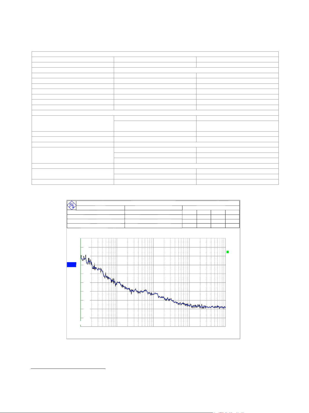
Measured phase noise of wideband analog I/Q outputs; single-ended sine wave with f = 100 MHz
15
The magnitude of the sum of output voltage and bias voltage must not exceed 4 V.
16
"Optimize internal I/Q impairments for RF output" switched off.
Running ...
R& S FSUP 50 Signal Source A nalyzer LO CKED
Set t ings Residual Noise [T1 w / o spurs] P hase Det ect or +40 dB
Signal F requenc y: 1 00 .0 00 0 0 2 MH z I nt P H N (10 0 .0 .. 1 .0 M ) -8 3 .3 dBc
Signal L ev el: 3 .22 dBm Res idual P M 5 .5 2 9 m°
C ros s C orr M ode H armonic 1 R es idual FM 1 0 .3 6 5 H z
I nternal Ref T uned I nternal P has e Det RM S Jitter 0 .15 3 6 ps
P has e Nois e [dBc /H z]
RF A tten 5 dB
T op - 8 0 dBc /Hz
1 kHz
10 kHz
100 kHz
100 Hz
1 MHz
-170
-160
-150
-140
-130
-120
-110
-100
-90
LoopBW 100 Hz
1 CLRW R
SMTH 1%
2 CLRW R
A
SPR OFF
TH 0dB
Frequency Offset
SMB100A Ser.No 175321
Date: 31.MAR.2003 05:52:13