SMW200A_specs_en_3606-8037-22_v2700.pdf - 第69页
Version 27.00, October 2024 Rohde & Schwar z R&S ® SMW200A Vec tor Signal Generator 69 Bandwidth extension ( R&S ® SMW -K555 option) The R&S ® SMW-K555 op tion require s two R&S ® SMW-B9 wide band bas…

Version 27.00, October 2024
68 Rohde & Schwarz R&S
®
SMW200A Vector Signal Generator
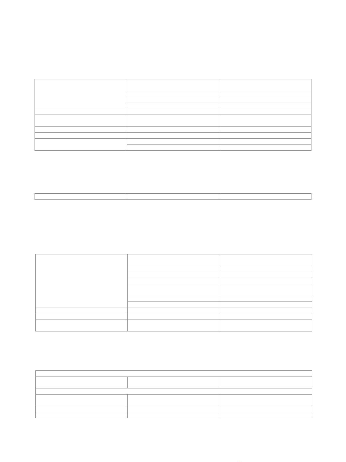
Crest factor reduction (R&S
®
SMW-K548 option)
Each R&S
®
SMW-K548 option requires a standard baseband generator (R&S
®
SMW-B10 option) or a wideband baseband generator
(R&S
®
SMW-B9 option). If two baseband generators are installed, crest factor reduction can be applied either on path A or B with one
R&S
®
SMW-K548 option. For crest factor reduction to be applied on paths A and B simultaneously, two R&S
®
SMW-K548 must be
installed.
Crest factor reduction can be applied to any waveform loaded in the arbitrary waveform generator.
State
on/off
Algorithm
clipping and filtering
Desired crest factor delta
–20 dB to 0 dB
Maximum iterations
1 to 10
Filter mode “simple”
Signal bandwidth
0 Hz to input file sample rate
Channel spacing
0 Hz to input file sample rate
Filter mode “enhanced”
Passband frequency
0 Hz to ½ of input file sample rate
Stopband frequency
0 Hz to ½ of input file sample rate
Maximum filter order
21 to 300
Slow I/Q (R&S
®
SMW-K551 option)
In slow I/Q mode, the generated signal’s clock rate can be reduced (e.g. a 20 MHz LTE signal is generated with a clock rate of
240 kHz instead of the original 30.72 MHz). This feature can be used to run tests on hardware emulation platforms not yet capable of
full-speed signal processing. The signal and fading characteristics are comparable to those of a system running at full speed. The
actual clock rate of the generated signal is controlled by the device connected to the digital I/Q output connectors of the
R&S
®
SMW200A.
R&S
®
SMW-K551 on instruments with wideband baseband (R&S
®
SMW-B9, R&S
®
SMW-B13XT)
At least one R&S
®
SMW-B9 wideband baseband generator option and one R&S
®
SMW-K19 digital baseband output for wideband
baseband option must be installed.
Note:
Only available for system configuration mode: advanced and signal outputs: digital only (HS).
All digital I/Q outputs need to run at the same clock rate.
The minimum clock rate is limited by the external controlling device only.
The R&S
®
SMW200A can handle varying clock rates.
With activated slow I/Q mode, marker signals are only available via the digital I/Q interface, and not via USER or T/M/C connectors.
With activated slow I/Q mode, no digital baseband inputs are available.
R&S
®
SMW-K551 on instruments with standard baseband (R&S
®
SMW-B10, R&S
®
SMW-B13/-B13T)
At least one R&S
®
SMW-B10 standard baseband generator option and one R&S
®
SMW-K18 digital baseband output option must be
installed.
Note:
All digital I/Q outputs need to run at the same clock rate.
The minimum clock rate is limited by the external controlling device only.
The R&S
®
SMW200A can handle varying clock rates.
In digital only/digital only multiplexed mode, marker signals are only available via the digital I/Q interface, and not via USER or T/M/C
connectors.
In digital only/digital only multiplexed mode with activated slow I/Q, no digital baseband inputs are available.
Version 27.00, October 2024
Rohde & Schwarz R&S
®
SMW200A Vector Signal Generator 69
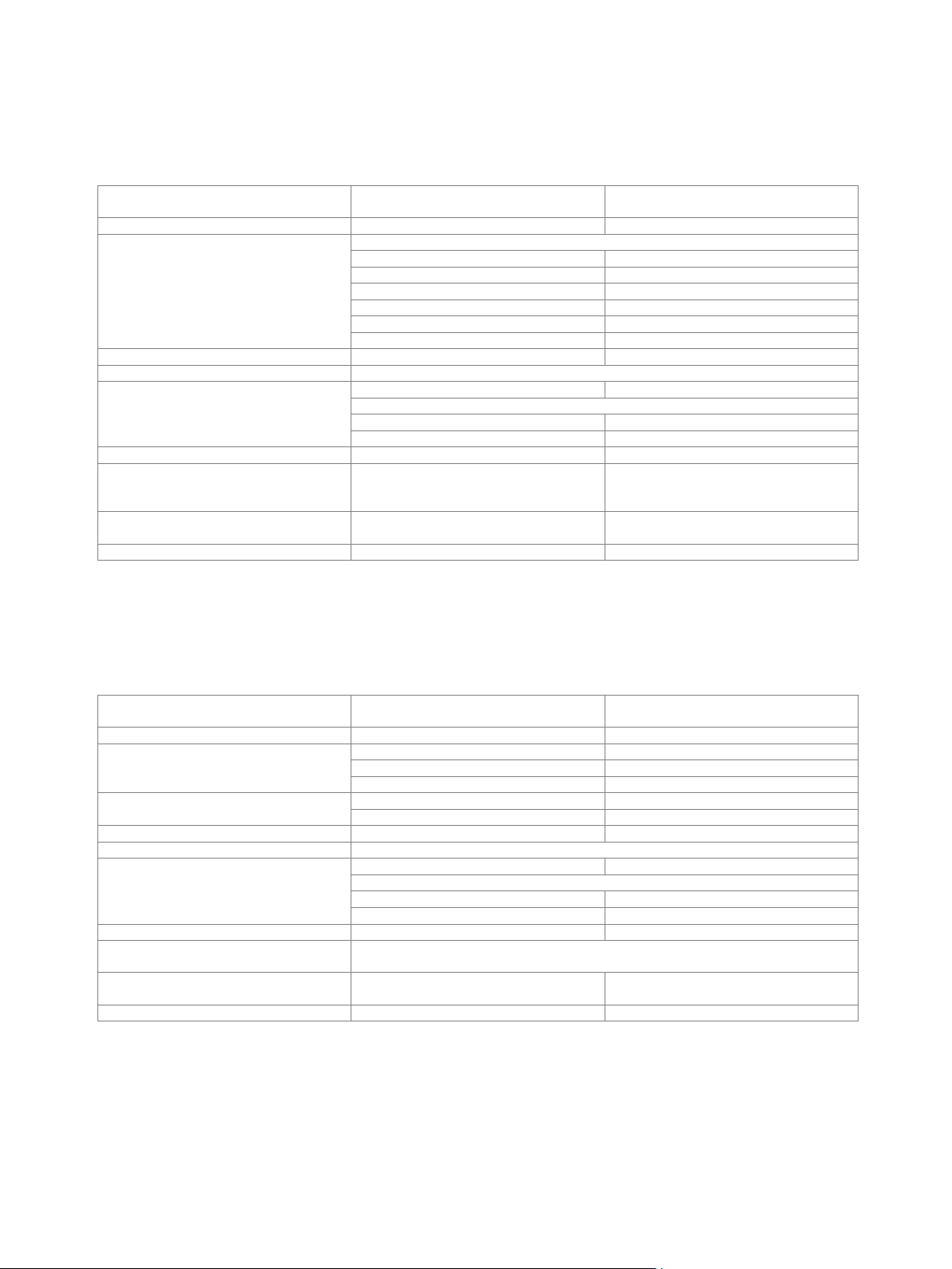
Bandwidth extension (R&S
®
SMW-K555 option)
The R&S
®
SMW-K555 option requires two R&S
®
SMW-B9 wideband baseband generator options and two R&S
®
SMW-K527 baseband
extension to 2 GHz RF bandwidth options. Single and dual unit operation is supported.
Bandwidth extension enhances the usable clock rate of the arbitrary waveform generator up to 4.8 GHz and can be used with any
waveform loaded int the arbitrary waveform generator. To run this option, an external power combiner and a measurement device is
needed. The measurement device can be either an analyzer or a power meter.
Supported standards and modulation
systems
with R&S
®
SMW-B9 option – arbitrary
waveform mode
ARB
with R&S
®
SMW-K414 option
OFDM
with R&S
®
SMW-K261 option
multicarrier CW
with R&S
®
SMW-K477 option
IEEE 802.11ay
State
on, off
Setup file
setup file including alignment data is
generated by bandwidth extension option
*.bwsa
Clock rate
200 MHz to 4.8 GHz
Bandwidth
up to 4 GHz
Waveform sample length
513 sample to 256 Msample
with R&S
®
SMW-K515 option
513 sample to 2 Gsample
Linearize RF (R&S
®
SMW-K575 option)
The R&S
®
SMW-K575 option requires at least one R&S
®
SMW-B10 standard baseband generator or R&S
®
SMW-B9 wideband
baseband generator.
Linearize RF improves the EVM and ACLR performance for high output powers over the whole RF frequency range of the device.
State
auto/off
Notched signals (R&S
®
SMW-K811 option)
At least one R&S
®
SMW-B10 standard baseband generator option or R&S
®
SMW-B9 wideband baseband generator option must be
installed. If two baseband generators are installed, notched signals can be generated either on path A or B with one R&S
®
SMW-K811
option. For notched signals to be generated on paths A and B simultaneously, two R&S
®
SMW-K811 must be installed.
Up to 25 band-stop filters can be applied to the baseband signal.
Center frequency and bandwidth can be set independently for each band-stop filter.
Supported standards and modulation
systems
with R&S
®
SMW-B9 or R&S
®
SMW-B10
option – arbitrary waveform mode
ARB
with R&S
®
SMW-K55 option
LTE
with R&S
®
SMW-K115 option
cellular IoT
with R&S
®
SMW-K114 option
custom OFDM
with R&S
®
SMW-K130 or
R&S
®
SMW-K355 option
OneWeb
with R&S
®
SMW-K52 option
DVB-H/DVB-T
with R&S
®
SMW-K116 option
DVB-S2/DVB-S2X
Number of notches
1 to 25
Notch width
0 Hz to 0.1 · clock frequency
Notch center frequency
–0.5 · clock frequency to +0.5 · clock
frequency
Customized digital input (R&S
®
SMW-K556 option)
With the R&S
®
SMW-K556 option, I/Q data from an existing hardware can be fed into the BBIN HS DIG I/Q inputs. This option can be
installed once or twice. Each R&S
®
SMW-K556 option to be installed requires a R&S
®
SMW-B9 wideband baseband generator option.
The existing hardware requires a Xilinx Virtex FPGA and the corresponding Rohde & Schwarz IP core.
Interface
Technical specifications
HS DIG I/Q interface input parameters
see section Digital baseband
inputs/outputs for wideband baseband
Interface parameters
Connector
HS DIG I/Q 1 and HS DIG I/Q 2 on rear
panel
QSFP+
Protocol
R&S
®
Digital I/Q Interface HS
Data rate
50 Gbit/s
sample rate up to 1.25 GHz
Version 27.00, October 2024
70 Rohde & Schwarz R&S
®
SMW200A Vector Signal Generator
BER measurement (R&S
®
SMW-K80 option)
At least one R&S
®
SMW-B10 standard baseband generator option or R&S
®
SMW-B9 wideband baseband generator option must be
installed.
The data supplied by the DUT is compared with a reference pseudo-random bit sequence.
Clock
supplied by DUT; a clock pulse is required
for each valid bit
Clock rate
100 Hz to 100 MHz
Data
PRBS
sequence length
9, 11, 15, 16, 20, 21, 23
pattern ignore
off, All 0, All 1
data enable
external
modes
off, high, low
restart
external
modes
on/off
Synchronization time
28 clock cycles
Interface
4 BNC connectors, selectable from USER 1 to 6
Clock, data, enable and restart inputs
input impedance
1 kΩ, 50 Ω
trigger threshold
setting range
0.1 V to 2.0 V
setting resolution
0.1 V
Polarity
data, clock, data enable
normal, inverted
Measurement time
selectable by means of maximum number
of data bits or bit errors (max. 2
31
bit
each), continuous measurement
Measurement result
if selected number of data bits or bit errors
is attained
BER in ppm, % or decade values
Status displays
not synchronized, no clock, no data
BLER measurement (R&S
®
SMW-K80 option)
At least one R&S
®
SMW-B10 standard baseband generator option or R&S
®
SMW-B9 wideband baseband generator option must be
installed.
In BLER measurement mode, arbitrary data can be provided by the DUT. A signal marking the block’s CRC has to be provided on the
data enable connector of the BER/BLER option.
Clock
supplied by DUT; a clock pulse is required
for each valid bit
Clock rate
100 Hz to 100 MHz
Data
input data
arbitrary
data enable (marking the block’s CRC)
external
modes
high, low
CRC
CRC type
CCITT CRC16 (x
16
+ x
12
+ x
5
+ 1)
CRC bit order
MSB first, LSB first
Synchronization time
1 block
Interface
4 BNC connectors, selectable from USER 1 to 6
Clock, data, and enable inputs
input impedance
1 kΩ, 50 Ω
trigger threshold
setting range
0.1 V to 2.0 V
setting resolution
0.1 V
Polarity
data, clock, data enable
normal, inverted
Measurement time
selectable by means of maximum number of received blocks or errors (max. 2
31
blocks
each), continuous measurement
Measurement result
if selected number of received blocks or
errors is attained
BLER in ppm, % or decade values
Status displays
not synchronized, no clock, no data