SOM-1735-001.pdf - 第12页
5.1.2 List of Individual Component Dat a The specific dat a for BGA/CSP component s are divided into two lists for the explanation. Fig. 5 B01 Shape Dat a T able 6 No. Component Shape BGA/CSP Ref. No. Remarks Dat a Name …
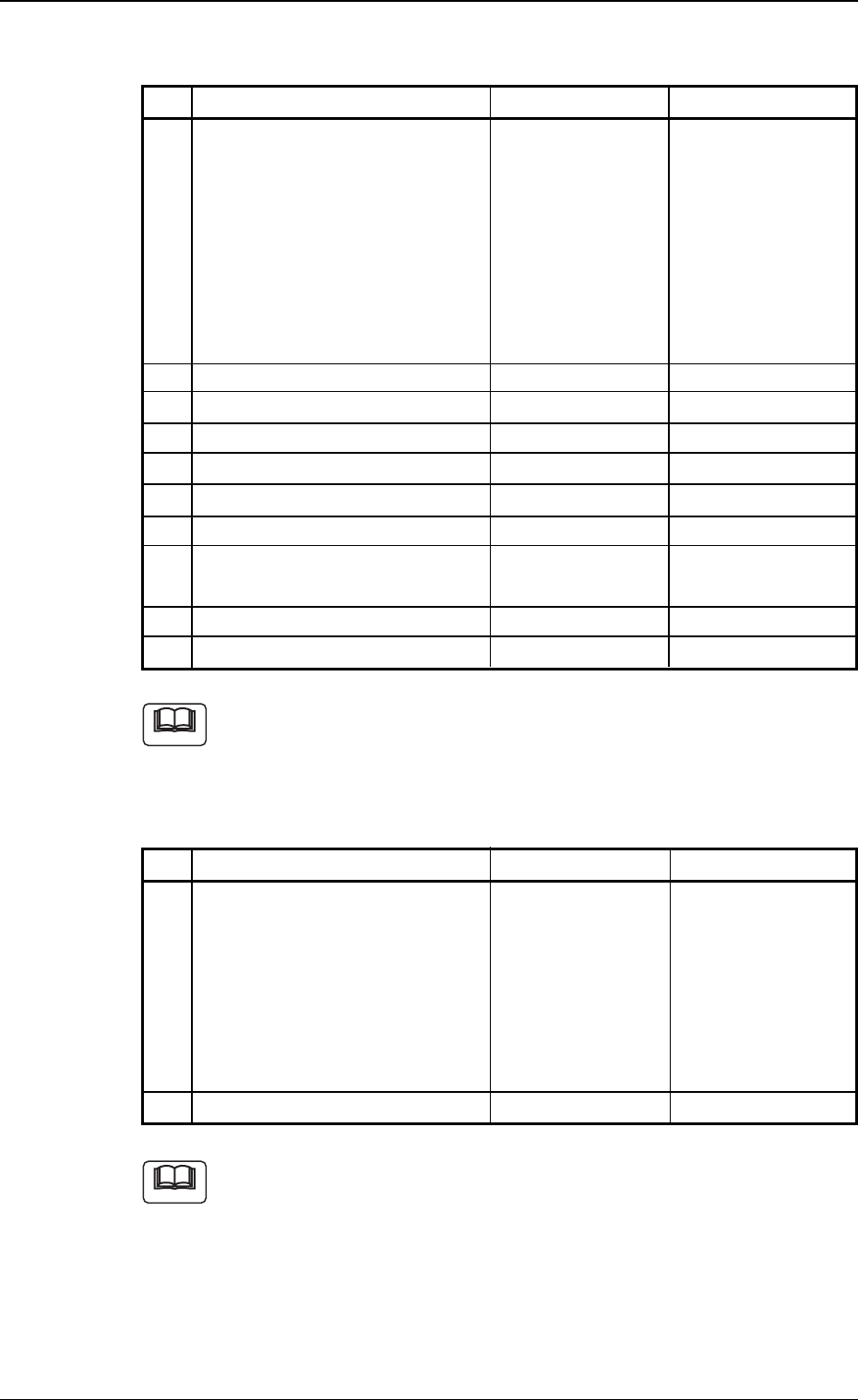
A02 List of Control Data
Table 4
No. Data Name Reference No. Remarks
1 Speed Data A02_01 See "Note" below.
(1) Pick-Up [sec]
(2) Rotary turret [sec]
(3) Placement [sec]
(4) X/Y table
(5) Feeder carriage
(6) Nozzle rotation
(7) Recognition time [sec]
2 Selected nozzle A02_02 See "Note" below.
3 Placement height feedback A02_03 See "Note" below.
4 Cmpnt thickness check [mm] A02_04 See "Note" below.
5 Vertical cmpnt data [mm] A02_05 See "Note" below.
6 Pickup level [mm] A02_06 See "Note" below.
7 Placement level [mm] A02_07 See "Note" below.
8 Pickup pos correction A02_08 See "Note" below.
X [mm], Y [mm]
9 Auto for axis adjustment X, Y A02_09 See "Note" below.
10 Error process 1, 2 A02_10 See "Note" below.
Refer to the instruction manual "Component Library for TCM-X Series"
for details.
A03 List of Carrier Data
Table 5
No. Data Name Reference No. Remarks
1 Carrier Data A03_01 See "Note" below.
(1) Type
(2) Tape width [mm]
(3) Tape feed pitch [mm]
(4) Tape feed counts
(5) Direction
(6) Q’ty
2 Tape end detection A03_02 See "Note" below.
Refer to the instruction manual "Component Library for TCM-X
Series" for details.
5.1 List of Data
Note
Note
0307-001 10 Tg0930-PM-SO
5.1.2 List of Individual Component Data
The specific data for BGA/CSP components are divided into two lists for
the explanation.
Fig. 5
B01 Shape Data
Table 6
No.
Component Shape
BGA/CSP Ref. No. Remarks
Data Name
1 Mold size B01_02
(1) X, Y
(2) T [mm] (thickness),
t [mm] (thickness),
Ut [mm] (thickness)
2 Polarity existence B01_04
3 Electrical Contact Data B01_11 See "Note" below.
(1) Grid Type
(2) Image
(3) # Of types
(4) # Of groups
(5) Extended setting
4 Electrode Type Data B01_12 See "Note" below.
(1) Shape
(2) Dim 1 [mm]
5 Electrode Group Data B01_13 See "Note" below.
(1) Type No.
(2) Gp Posn X [mm],
Y [mm]
(3) # Of Rows, # Of Cols
(4) Row Pitch [mm],
Col Pitch [mm]
(5) Missing Elctd Set
(6) # of Missing Blocks
6 Missing Electrode Data B01_14 See "Note" below.
(1) Missing Stg Row,
Missing Stg Col
(2) # Of Missing Rows
[pcs.],
# Of Missing Cols
[pcs.]
The data is exclusively used for BGA/CSP components.
5.1 List of Data
• Area Array
"BGA/CSP"
B01 List of Shape Data
B02 List of Recognition Data
List of Individual Component Data
Note
0307-001 11 Tg0930-PM-SO
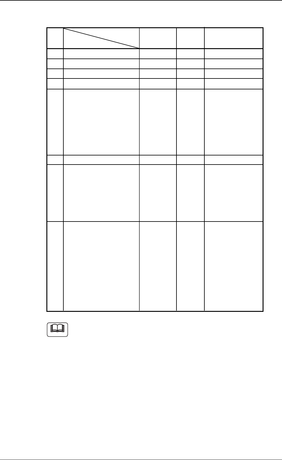
B02 Recognition Data
Table 7
No.
Component Shape
BGA/CSP Ref. No. Remarks
Data Name
1 Lighting mode B02_01
2 Recog data set B02_02
3 Recog level B02_03
4 Front recognition ltg algo B02_04
5 Lighting pattern B02_05
(1) Lighting pattern
selection
(2) Back ltg
(3) Front ltg 1 (Ring)
(4) Front ltg 2 (Coax)
(5) Front ltg 3 (Ring) See "Note" below.
6 View Range Set B02_06
7 Electrode Recognition B02_13
Data
(1) Elctd pos detn
(2) Elctd pos tol [mm]
(3) Electd size detn
(4) Electd size tol [mm]
8 Polarity Determination B02_14 See "Note" below.
Data
(1) Polarity detn
(2) Inspection method
(3) Inspection pos
X [mm], Y [mm]
(4) Inspection range
[mm]
(5) Inspection range
image
The data is exclusively used for BGA/CSP components.
5.1 List of Data
Note
0307-001 12 Tg0930-PM-SO