D4+circuit(2006).pdf - 第145页
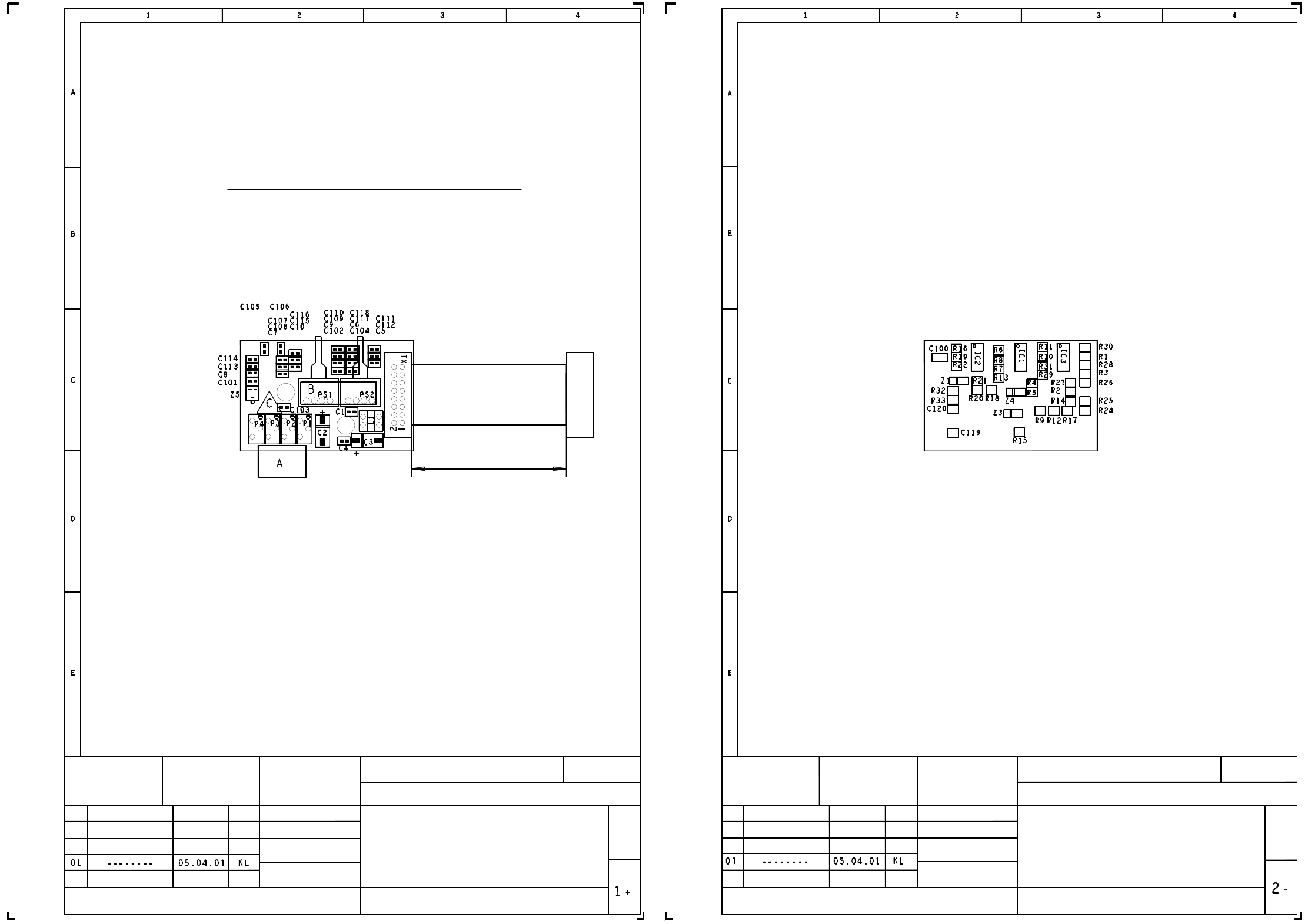
5 - 15 0036707 4-010 102ND4 Adjus tment u nit 3 , placem ent cir cuit 0300228 0-020 101ND4 PCB 1028, vision DC / DC con verter 003 6707 4-010102N D4 1 1 SIEMENS AG 06.11.2001 06.03.06 US02 Date Name Date Name U1 X1 R5 R6…
5 - 14
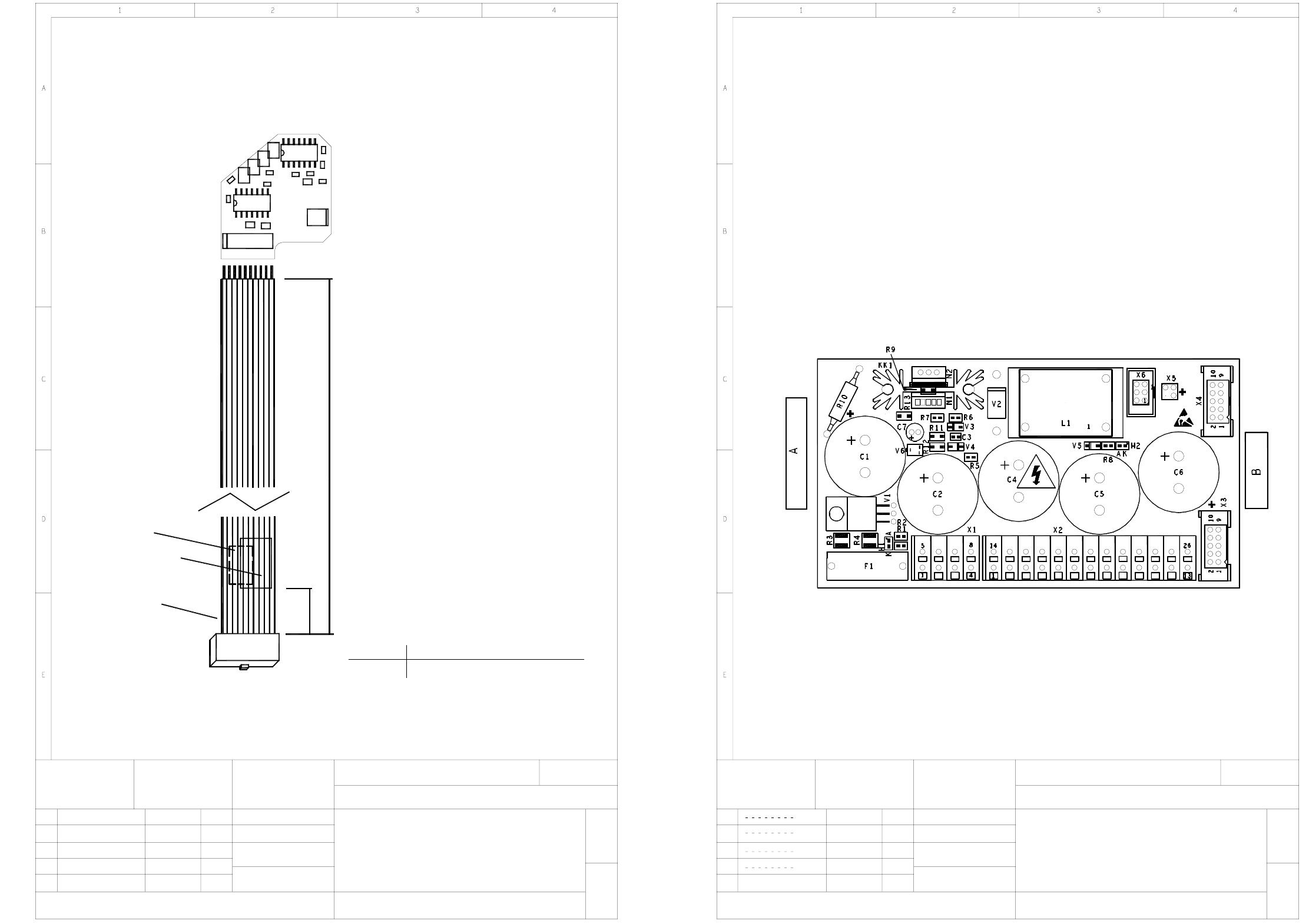
00363738-020101ND4 PCB 983, vacuum board (2 meas. ranges) (sh. 1 of 2)
00363738-020101ND4 PCB 983, vacuum board (2 meas. ranges) (sh. 2 of 2)
pflichten zu Schadenersatz. Alle Rechte vorbehalten, ins
besondere für den Fall der Patenterteilung oder GM-Eintragung
wertung und Mitteilung ihres Inhalts nicht gestattet, soweit
Weitergabe sowie Vervielfältigung dieser Unterlage,Ver-
nicht ausdrücklich zugestanden. Zuwiderhandlungen ver-
Proprietary date, company confidential. All rights reserved.
Confie a titre de secret d'entreprise. Tous droits reserves.
Confiado como secrete industrial. Nos reservamos todos los derechos.
Comunicado como segredo empresarial. Reservados todos os direitos.
00363738-020101ND4
G32918-N0031-U501-*-0017
C = ESD-LABEL
B = INSPECTION LABEL ON PRESSURE SENSORS
A = IDENTIFICATION LABEL, LATERAL TO P1-P4
Sheet
X1
Connector
X10*c gantry head distributor 03038002
Assembly
KLOSE
05.04.01
VACUUM BOARD (2 MEAS. RANGES)
PCB 983
Placement diagram component side
4-layer PCB
Scale 1:1
Name
Date
NameDateNote
Status
SIEMENS AG
Copyright reserved
pflichten zu Schadenersatz. Alle Rechte vorbehalten, ins
besondere für den Fall der Patenterteilung oder GM-Eintragung
wertung und Mitteilung ihres Inhalts nicht gestattet, soweit
Weitergabe sowie Vervielfältigung dieser Unterlage,Ver-
nicht ausdrücklich zugestanden. Zuwiderhandlungen ver-
Proprietary date, company confidential. All rights reserved.
Confie a titre de secret d'entreprise. Tous droits reserves.
Confiado como secrete industrial. Nos reservamos todos los derechos.
Comunicado como segredo empresarial. Reservados todos os direitos.
G32918-N0031-U501-*-0017
00363738-020101ND4
VACUUM BOARD (2 MEAS. RANGES)
05.04.01
KLOSE
Status
Note Date
Date
Name
Name
Placement diagram component side
4-layer PCB
PCB 983
Scale 1:1
Sheet
Copyright reserved
SIEMENS AG
5 - 15
00367074-010102ND4 Adjustment unit 3, placement circuit
03002280-020101ND4 PCB 1028, vision DC / DC converter
00367074-010102ND4
1
1
SIEMENS AG
06.11.2001
06.03.06US02
Date Name
Date
Name
U1
X1
R5
R6
Pin 1
X1
A1
B1, B2
1
10
R
1
X2
C3
X3
R4
U2
X5
X4
R2
R3
+5.0mm
-5.0mm
50.0mm
354.0mm
B1, B2:
A1:
C2
U3
R7
C4
C5
C6
Cable, 05-1630-5
X18*c gantry head distributor 03038002
Assembly
Connector
X1
on the cable
Readable, when X1 is on the right.
50mm distance from cable end.
AFO and WIP inspection labels.
Label position:
On the back.
Identification label,
readable, when X1 is on the left.
May be printed
pflichten zu Schadenersatz. Alle Rechte vorbehalten, ins
besondere für den Fall der Patenterteilung oder GM-Eintragung
wertung und Mitteilung ihres Inhalts nicht gestattet, soweit
Weitergabe sowie Vervielfältigung dieser Unterlage,Ver-
nicht ausdrücklich zugestanden. Zuwiderhandlungen ver-
Proprietary date, company confidential. All rights reserved.
Confie a titre de secret d'entreprise. Tous droits reserves.
Confiado como secrete industrial. Nos reservamos todos los derechos.
Comunicado como segredo empresarial. Reservados todos os direitos.
402386 TB
Mayerhofer
Copyright reserved
SIPLACE D4
Stat. Modification
Adjustment drive 3
Placement circuit
Sheet
Sh.
Stat.
01.
03.
02.
Modified
21.01.02
19.04.02
30.07.02
Date
EN
EN
KL
Name
Date
Name
21.01.02
KLOSE
G32905 - N0117 - U021 - * - 0017
03002280-020101ND4
VISION DC / DC CONVERTER
PCB 1028
2-LAYER PCB
COMPONENT LAYOUT, COMPONENT SIDE
Scale 1 : 1
Sheet
1 -
C = ESD label
Glue "lightning" label on C4
B = inspection label on C6
A = identification label on C1
pflichten zu Schadenersatz. Alle Rechte vorbehalten, ins
besondere für den Fall der Patenterteilung oder GM-Eintragung
wertung und Mitteilung ihres Inhalts nicht gestattet, soweit
Weitergabe sowie Vervielfältigung dieser Unterlage,Ver-
nicht ausdrücklich zugestanden. Zuwiderhandlungen ver-
Proprietary date, company confidential. All rights reserved.
Confie a titre de secret d'entreprise. Tous droits reserves.
Confiado como secrete industrial. Nos reservamos todos los derechos.
Comunicado como segredo empresarial. Reservados todos os direitos.
04. 18.07.03 EN
EDM D&D MCH
Copyright reserved
SIEMENS AG
5 - 16
03003536-010101ND4 TQM 167 SIPLACE embedded module
Alternating display of "I-" and "-I"
Sequence of numbers (3 digits) flashing
Point flashing
No display
"P" for PROGRAM
"E" for ERASE
Circulating segments
"b" flashing
Undefined display
7-segment display
Application
BIOS
Jump to application (approx. 5 s)
No application available
Error in operating system
No error after Reset
Download executing
Delete flash
Program flash
Reset error
No FW available
Status Modified Date NameNorm
Check.
Author
Date
TQM167 Siplace Embedded Module
SIPLACE SMD Placement System
Sh.
Sheet
C = Function test designation
B = Identification
A = ESD label
DS01 New
X1
X1
X2
1
280
79
120
119
2
1
SIPLACE D4
11.06.02 TB
03003536-010101ND4
11.06.2002
Bichler
Copyright reserved
Designer 7.1
SIEMENS AG