IPC-SM-782A 表面安装设计和焊盘设计标准(带BGA).pdf - 第104页
4.0 COMPONENT DIMENSIONS Figure 2 provides the component dimensions for SOT 143 components. Component Identifier L (mm) S (mm) W1 (mm) W2 (mm) T (mm) P1 (mm) P2 (mm) H (mm) min max min max min max min max min max basic ba…
1.0 SCOPE
This subsection provides the component and land pattern
dimensions for SOT 143 (small outline transistor) components.
Basic construction of the SOT 143 device is also covered. At
the end of this subsection is a listing of the tolerances and
target solder joint dimensions used to arrive at the land pat-
tern dimensions.
2.0 APPLICABLE DOCUMENTS
See Section 8.0 for documents applicable to the subsections.
2.1 Electronic Industries Association (EIA)
JEDEC Pub-
lication 95 Registered and Standard Outlines for Solid State
and Related Products, TO-253, Issue ‘‘C’’ dated 11/14/90
Application for copies should be addressed to:
Global Engineering Documents
1990 M Street N.W.
Washington, DC
3.0 COMPONENT DESCRIPTIONS
These parts are for dual diodes and Darlington transistors.
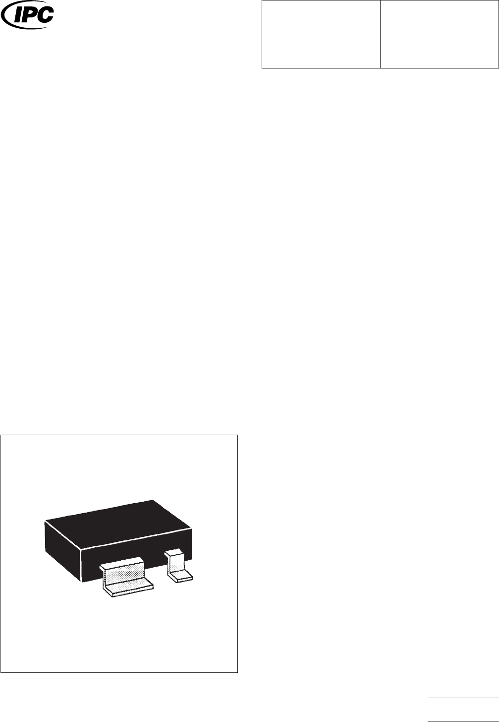
3.1 Basic Construction
See Figure 1. The dimensional
characteristics are designed to meet the needs of the surface
mount industry. The clearance between the body of the com-
ponent and the packaging and interconnect structure is speci-
fied at 0.05 to 0.13 mm [0.002 to 0.005 in] to accommodate
reflow or wave soldering processes.
3.1.1 Termination Materials
Leads must be solder-
coated with a tin/lead alloy. The solder should contain
between 58 to 68% tin. Solder may be applied to the leads by
hot dipping or by plating from solution. Plated solder termina-
tions should be subjected to post-plating reflow operation to
fuse the solder. The tin/lead finish should be at least 0.0075
mm [0.0003 in] thick.
Solder finish applied over precious metal electrodes should
have a diffusion barrier layer between the electrode metalliza-
tion and the solder finish. The barrier layer should be nickel or
an equivalent diffusion barrier, and should be at least 0.00125
mm [0.00005 in] thick.
3.1.2 Marking
Parts are available with or without marked
values.
3.1.3 Carrier Package Format
Carrier package format
shall be according to the following: body type TO-253, 8 mm
tape/4 mm pitch.
3.1.4 Resistance to Soldering
Parts should be capable of
withstanding five cycles through a standard reflow system
operating at 215°C. Each cycle shall consist of 60 seconds
exposure at 215°C. Parts must also be capable of withstand-
ing a minimum of 10 seconds immersion in molten solder at
260°C.
IPC-782-8-9-1
Figure 1 SOT 143 construction
IPC-SM-782
Surface Mount Design
and Land Pattern Standard
Date
8/93
Section
8.9
Revision Subject
SOT 143
Page1of4
电子技术应用 www.ChinaAET.com
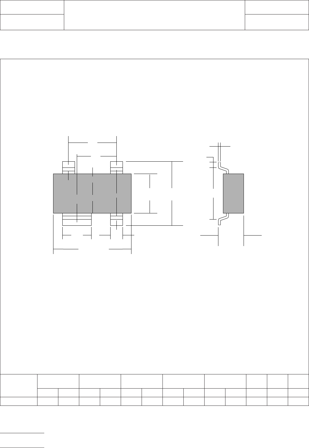
4.0 COMPONENT DIMENSIONS
Figure 2 provides the component dimensions for SOT 143 components.
Component
Identifier
L (mm) S (mm) W1 (mm) W2 (mm) T (mm)
P1
(mm)
P2
(mm)
H
(mm)
min max min max min max min max min max basic basic max
SOT 143 2.10 2.64 1.00 1.69 0.37 0.46 0.76 0.89 0.25 0.55 1.92 1.72 1.20
Figure 2 SOT 143 component dimensions
▼
▼
▼
▼
▼
▼
▼
▼
▼
▼
▼
P2
P1
▼
▼
▼▼
L
1.20–1.40
2.80–3.04
W1
W2
▼
▼
H
S
▼
▼
▼
0.85–0.130
▼
▼
T
IPC-782-8-9-2
IPC-SM-782
Subject
SOT 143
Date
8/93
Section
8.9
Revision
Page2of4
电子技术应用 www.ChinaAET.com
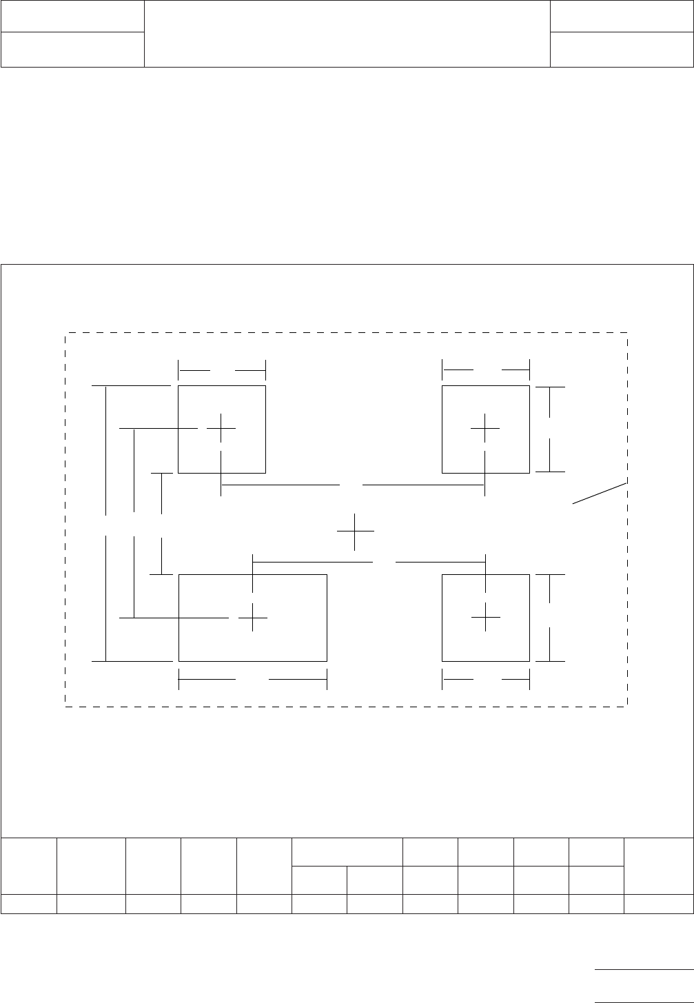
5.0 LAND PATTERN DIMENSIONS
Figure 3 provides the land pattern dimensions for SOT 143
components. These numbers represent industry consensus
on the best dimensions based on empirical knowledge of fab-
ricated land patterns.
In the table, the dimensions shown are at maximum material
condition (MMC). The least material condition (LMC) should
not exceed the fabrication (F) allowance shown on page 4.
The LMC and the MMC provide the limits for each dimension.
The dotted line in Figure 3 shows the grid placement court-
yard which is the area required to place land patterns and
their respective components in adjacent proximity without
interference or shorting. Numbers in the table represent the
number of grid elements (each element is 0.5 by 0.5 mm) in
accordance with the international grid detailed in IEC publica-
tion 97.
RLP No.
Component
Identifier Z (mm) G (mm) X1 (mm)
X2 (mm) C E1 E2 Y
Placement
Grid (No.
of Grid
elements)min max ref Basic Basic ref
225 SOT 143 3.60 0.80 1.00 1.00 1.20 2.20 1.90 1.70 1.40 8x8
Figure 3 SOT 143 land pattern dimensions
▼
▼
▼
▼
▼
▼
▼
▼
▼
▼
C
E2
Y
X1X2
Grid
Placement
Courtyard
▼
G
▼
▼
▼
▼
Y
▼
▼
X1
▼
▼
E1
▼
▼
X1
Z
▼
▼
IPC-782-8-9-3
IPC-SM-782
Subject
SOT 143
Date
8/93
Section
8.9
Revision
Page3of4
电子技术应用 www.ChinaAET.com