IPC-SM-782A 表面安装设计和焊盘设计标准(带BGA).pdf - 第166页
6.0 TOLERANCE AND SOLDER JOINT ANALYSIS Figure 4 provides an analysis of tolerance assumptions and resultant solder joints based on the land pattern dimensions shown in Figure 3. Tolerances for the component dimensions, …
RLP
No. Component Identifier
Z1
(mm)
G1
(mm)
Z2
(mm)
G2
(mm) X (mm)
Y (mm)
C1
(mm)
D1
(mm)
C2
(mm)
D2
(mm) E (mm)
Placement Grid
(No. of Grid
Elements)ref ref ref ref ref ref
710A QFP 14X20-80 18.00 14.40 24.00 20.40 0.50 1.80 16.20 12.00 22.20 18.40 0.80 38x50
711A QFP 14X20-100 18.00 14.40 24.00 20.40 0.40 1.80 16.20 12.35 22.20 18.85 0.65 38x50
712A SQFP 14X20-120 16.80 13.60 22.80 19.60 0.30 1.60 15.20 11.50 21.20 17.50 0.50 36x48
713A SQFP 14X20-128 16.80 13.60 22.80 19.60 0.30 1.60 15.20 12.50 21.20 18.50 0.50 36x48
714A SQFP 14X20-152 16.80 13.60 22.80 19.60 0.25 1.60 15.20 11.60 21.20 18.00 0.40 36x48
715A SQFP 14X20-160 16.80 13.60 22.80 19.60 0.25 1.60 15.20 12.40 21.20 18.80 0.40 36x48
716A SQFP 14X20-208 16.80 13.60 22.80 19.60 0.17 1.60 15.20 12.30 21.20 18.30 0.30 36x48
717A SQFP 14X20-216 16.80 13.60 22.80 19.60 0.17 1.60 15.20 12.90 21.20 18.90 0.30 36x48
720A SQFP 20X28-176 22.80 19.60 30.80 27.60 0.30 1.60 21.20 17.50 29.20 25.50 0.50 48x66
721A SQFP 20X28-184 22.80 19.60 30.80 27.60 0.30 1.60 21.20 18.50 29.20 26.50 0.50 48x66
722A SQFP 20X28-224 22.80 19.60 30.80 27.60 0.25 1.60 21.20 18.00 29.20 26.00 0.40 48x66
723A SQFP 20X28-232 22.80 19.60 30.80 27.60 0.25 1.60 21.20 18.80 29.20 26.80 0.40 48x66
724A SQFP 20X28-300 22.80 19.60 30.80 27.60 0.17 1.60 21.20 18.30 29.20 26.10 0.30 48x66
725A SQFP 20X28-308 22.80 19.60 30.80 27.60 0.17 1.60 21.20 18.90 29.20 26.70 0.30 48x66
730A SQFP 28X40-256 30.80 27.60 42.80 39.60 0.30 1.60 29.20 25.50 41.20 37.50 0.50 66x88
731A SQFP 28X40-264 30.80 27.60 42.80 39.60 0.30 1.60 29.20 26.50 41.20 38.50 0.50 66x88
732A SQFP 28X40-324 30.80 27.60 42.80 39.60 0.25 1.60 29.20 26.00 41.20 38.00 0.40 66x88
733A SQFP 28X40-332 30.80 27.60 42.80 39.60 0.25 1.60 29.20 26.80 41.20 38.80 0.40 66x88
734A SQFP 28X40-432 30.80 27.60 42.80 39.60 0.17 1.60 29.20 26.10 41.20 38.10 0.30 66x88
735A SQFP 28X40-440 30.80 27.60 42.80 39.60 0.17 1.60 29.20 26.70 41.20 38.70 0.30 66x88
Figure 3b SQFP/QFP (Rectangular) land pattern dimensions
Y
X
Full radius
optional
▼
▼
▼
▼
▼
Z2
G2
▼
▼
▼
▼
E
▼
▼
C2
▼
▼
C1
G1 Z1
▼
▼
▼
▼
▼
▼
▼
Grid
placement courtyard
D2
▼
▼
D1
▼
▼
IPC-782-11-3-3b
IPC-SM-782
Subject
SQFP/QFP (Rectangular)
Date
5/96
Section
11.3
Revision
A
Page5of6
电子技术应用 www.ChinaAET.com
6.0 TOLERANCE AND SOLDER JOINT ANALYSIS
Figure 4 provides an analysis of tolerance assumptions and
resultant solder joints based on the land pattern dimensions
shown in Figure 3. Tolerances for the component dimensions,
the land pattern dimensions (fabrication tolerances on the
interconnecting substrate), and the component placement
equipment accuracy are all taken into consideration.
Figure 4 provides the solder joint minimums for toe, heel, and
side fillets, as discussed in Section 3.3. The tolerances are
addressed in a statistical mode, and assume even distribution
of the tolerances for component, fabrication, and placement
accuracy.
Individual tolerances for fabrication (‘‘F’’) and component
placement equipment accuracy (‘‘P’’) are assumed to be as
given in the table. These numbers may be modified based on
user equipment capability or fabrication criteria. Component
tolerance ranges (C
L
,C
S
, and C
W
) are derived by subtracting
minimum from maximum dimensions given in Figure 2. The
user may also modify these numbers, based on experience
with their suppliers. Modification of tolerances may result in
alternate land patterns (patterns with dimensions other than
the IPC registered land pattern dimensions).
The dimensions for minimum solder fillets at the toe, heel, or
side (J
T
,J
H
,J
S
) have been determined based on industry
empirical knowledge and reliability testing. Solder joint
strength is greatly determined by solder volume. An observ-
able solder fillet is necessary for evidence of proper wetting.
Thus, the values in the table usually provide for a positive sol-
der fillet. Nevertheless, the user may increase or decrease the
minimum value based on process capability.
RLP No.
Tolerance
Assumptions (mm)
Solder Joint (Sides 1 and 2)
Toe (mm) Heel (mm) Side (mm)
FPC
L
J
T
min J
T
max C
S
J
H
min J
H
max C
W
J
S
min J
S
max
680/681A 0.10 0.10 0.49 0.29 0.50 0.75 0.29 0.65 0.35 -0.02 0.10
682/683A 0.10 0.10 0.49 0.29 0.50 0.75 0.29 0.65 0.33 -0.01 0.10
684/685A 0.10 0.10 0.49 0.29 0.50 0.75 0.29 0.65 0.30 -0.03 0.06
690/691A 0.10 0.10 0.49 0.29 0.50 0.75 0.29 0.65 0.35 -0.02 0.10
692/693A 0.10 0.10 0.49 0.29 0.50 0.75 0.29 0.65 0.33 -0.01 0.10
694/695A 0.10 0.10 0.49 0.29 0.50 0.75 0.29 0.65 0.30 -0.03 0.06
700/701A 0.10 0.10 0.49 0.29 0.50 0.75 0.29 0.65 0.35 -0.02 0.10
702/703A 0.10 0.10 0.49 0.29 0.50 0.75 0.29 0.65 0.33 -0.01 0.10
704/705A 0.10 0.10 0.49 0.29 0.50 0.75 0.29 0.65 0.30 -0.03 0.06
710A 0.10 0.10 0.57 0.27 0.53 0.76 0.22 0.58 0.32 -0.00 0.10
711A 0.10 0.10 0.57 0.27 0.53 0.76 0.22 0.58 0.33 -0.02 0.09
712/713A 0.10 0.10 0.49 0.29 0.50 0.75 0.29 0.65 0.35 -0.02 0.10
714/715A 0.10 0.10 0.49 0.29 0.50 0.75 0.29 0.65 0.33 -0.01 0.10
716/717A 0.10 0.10 0.49 0.29 0.50 0.75 0.29 0.65 0.30 -0.03 0.06
720/721A 0.10 0.10 0.49 0.29 0.50 0.75 0.29 0.65 0.35 -0.02 0.10
722/723A 0.10 0.10 0.49 0.29 0.50 0.75 0.29 0.65 0.33 -0.01 0.10
724/725A 0.10 0.10 0.49 0.29 0.50 0.75 0.29 0.65 0.30 -0.03 0.06
730/731A 0.10 0.10 0.49 0.29 0.50 0.75 0.29 0.65 0.35 -0.02 0.10
732/733A 0.10 0.10 0.49 0.29 0.50 0.75 0.29 0.65 0.33 -0.01 0.10
734/735A 0.10 0.10 0.49 0.29 0.50 0.75 0.29 0.65 0.30 -0.03 0.06
Figure 4 Tolerance and solder joint analysis
Zmax
Lmin
▼
▼
▼
▼
1
/2 T
T
J
T
min
Smax
J
H
min
1
/2 T
H
Xmax
▼
▼
Toe Fillet
▼
▼
▼
Heel Fillet
Side Fillet
▼
▼
▼
▼
▼
J
T
max
J
H
max
J
S
min
▼
▼
▼
▼
▼
▼
▼
▼
▼
▼
▼
▼
▼
▼
▼
Gmin
▼
1
/2 T
S
J
S
max
▼
▼
▼
Wmin
▼
IPC-782-11-3-4
IPC-SM-782
Subject
SQFP/QFP (Rectangular)
Date
5/96
Section
11.3
Revision
A
Page6of6
电子技术应用 www.ChinaAET.com
1.0 SCOPE
This subsection provides the component and land pattern
dimensions for ceramic quad flat pack (CQFP) components.
Basic construction of the CQFP device is also covered. At the
end of this subsection is a listing of the tolerances and target
solder joint dimensions used to arrive at the land pattern
dimensions.
2.0 APPLICABLE DOCUMENTS
JEDEC Publication 95
Registered and Standard Outlines for
Solid JEDEC Publication 95 State and Related Products, Out-
line MS 044
3.0 COMPONENT DESCRIPTIONS
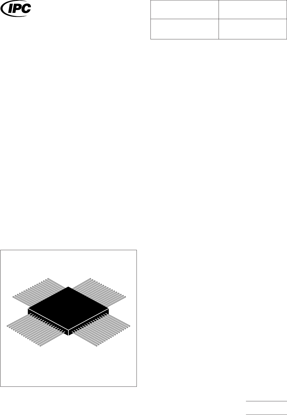
3.1 Basic Construction
See Figure 1. Leaded ceramic
chip carriers are typically supplied with an open cavity for chip
placement. Ceramic or metal lids are soldered, epoxied, or
attached with glass frit around the cavity to provide a hermetic
seal.
An exception to this construction is the JEDEC standard
MS044, which has the chip bonded to a lead frame, which is
then sealed between two ceramic bodies with glass frit, simi-
lar to CERDIP fabrication. The ceramic packages are available
in 28- through 196-lead configurations, with 1.27, 0.80, and
0.64 mm center spacing.
Pre-leaded ceramic chip carriers typically have copper alloy or
Kovar leads that are attached by the manufacturer. Leads are
typically bonded to metallization on the top surface of the chip
carrier. However, leads can be attached to the package cas-
tellations as well. Brazing or thermocompression bonding is
usually the attachment means.
Pre-leaded packages using lead-frame construction are also
available. These chip carriers have ceramic bodies with two
opposing halves which mate above and below a lead frame to
which the chip has been previously bonded. The seal is pre-
formed with glass frit.
Leads can be formed to different shapes, such as ‘‘J,’’ ‘‘L,’’
or ‘‘C’’ configurations. Leads bent in the ‘‘L’’ configuration are
known as ‘‘gullwings.’’
Pre-leaded chip carriers may be supplied with leads straight
and attached to a common strip. The user must detach the
common strip and form the leads to the desired configuration.
This is done to minimize lead bending during shipping and
handling. Leads may be supplied pre-tinned or with gold plat-
ing, as is often done for packages intended for a high reliabil-
ity user.
3.1.1 Termination Materials
Leads must be solder-
coated with a tin/lead alloy. The solder should contain
between 58 to 68% tin. Solder may be applied to the leads by
hot dipping or by plating from solution. Plated solder termina-
tions should be subjected to post-plating reflow operation to
fuse the solder. The tin/lead finish should be at least 0.0075
mm [0.0003 in] thick.
3.1.2 Marking
All parts shall be marked with a part number
and ‘‘Pin 1’’ location. Pin 1 location may be molded into the
plastic body.
3.1.3 Carrier Package Format
Tube carriers are preferred
for best handling.
3.1.4 Process Considerations
CQFPs are usually pro-
cessed using standard solder reflow processes. Parts should
be capable of withstanding ten cycles through a standard
reflow system operating at 215°C. Each cycle shall consist of
60 seconds exposure at 215°C.
IPC-782-11-4-1
CQFP construction
IPC-SM-782
Surface Mount Design
and Land Pattern Standard
Date
5/96
Section
11.4
Revision
A
Subject
CQFP
Page1of4
电子技术应用 www.ChinaAET.com