IPC-SM-782A 表面安装设计和焊盘设计标准(带BGA).pdf - 第22页
basic dimension of the spacing of one component lead ter- mination or castellation to its adjacent counterpart(s). No tolerance is assigned to pitch in the profile dimensioning concept. Dif ferences in pitch shall be incl…
Therefore, the calculations for ‘‘S’’ minimum and maxi-
mum dimensions are as follows:
S
min
=L
min
–2T
max
= 5.8 – 2(1.27) = 3.26
S
max
=L
max
–2T
min
= 6.2 – 2(0.4) = 5.4 mm
S
tol
=S
max
–S
min
= 5.4 – 3.26 = 2.14 mm
The difference between S
min
and S
max
is 2.14 mm,
which is probably a larger tolerance range than the
actual range within which these components are manu-
factured. This worst-cast scenario for the tolerance
range for ‘‘S’’ can also be calculated by adding the tol-
erances for the component length and the two terminals:
S
tol
=L
tol
+2T
tol
= 0.4 + 2(0.87) = 2.14 mm
In order to arrive at a more realistic tolerance range, the
RMS (root-mean-square) value is calculated using the
tolerances on the dimensions involved (‘‘L’’ and ‘‘T’’):
S
tol
(rms) =(L
tol
)
2
+ 2(T
tol
)
2
=
√
0.4
2
+ 2(0.87)
2
= 1.29mm
S
tol
(rms) is added to S
min
to arrive at a maximum ‘‘S’’
dimension. This technique is used so that a more realis-
tic S
max
dimension is used in the land pattern equations
for calculating G
min
(minimum land pattern gap between
heel fillets). In this example, the following calculation is
used for S
max
:
S
max
(rms) = S
min
+S
tol
(rms) = 3.26 + 1.29 = 4.55 mm
To determine the G
min
dimension for the land pattern,
S
tol
(rms) is used for the component tolerance (i.e., S
tol
(rms) = ‘‘C’’). The calculations for G
min
are as follows:
G
min
=S
max
–2J–
√
C
2
+ F
2
+ P
2
Where:
J = 0.5 mm (target heel fillet)
C=S
tol
(rms) = 1.29 mm (see above calculations from
component dimensions)
F = 0.1 mm (assumed fabrication tolerance)
P = 0.1 mm (assumed assembly equipment placement
tolerance)
Therefore:
G
min
=4.55–2(0.5) –
√
(1.29)
2
+(0.1)
2
+(0.1)
2
= 2.25 mm
Another major condition for multiple-leaded components
that must be considered in land pattern design is lead, ter-
mination, or castellation pitch. The pitch describes the
IPC-782-3-5
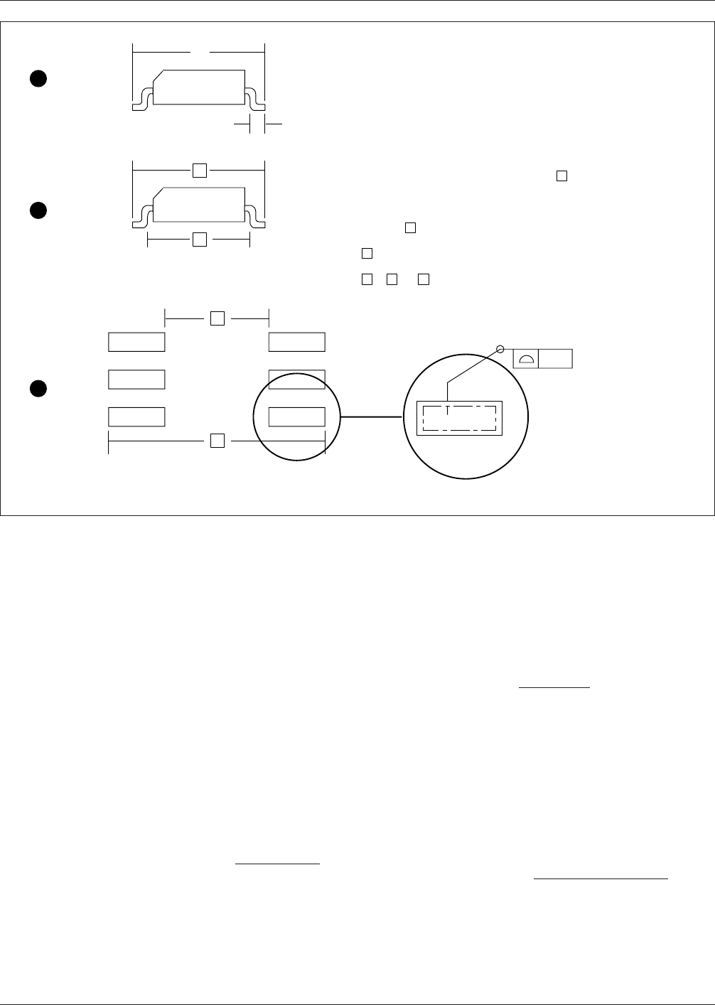
Figure 3–5 Profile dimensioning of a gullwing leaded SOIC
L
▼
▼
▼
▼
T
L
▼
▼
S
MMC
▼
▼
G
▼
▼
▼
Z
▼
▼
▼
0.05
"
N
"
Places
Fabrication tolerance
equals 0.1
mm
Manufacturers dimensions and tolerances
converted to profile dimensions, with S
at "maximum material condition".
Note: if S is not provided by the component
manufacturer it may be determined by subtracting
T terminal dimensions from the length.
S = L - 2 T
Manufacturing dimensions of SOIC's
A
B
C
MMC MMC LMC
December 1999 IPC-SM-782A
13
电子技术应用 www.ChinaAET.com

basic dimension of the spacing of one component lead ter-
mination or castellation to its adjacent counterpart(s). No
tolerance is assigned to pitch in the profile dimensioning
concept. Differences in pitch shall be included in the width
dimensions of the lead, termination, or castellation which
are dimensioned as basic at the minimum size.
3.3.2 Land Tolerancing
Profile tolerancing is used for
lands in a manner similar to that of the components. All
tolerances for lands are intended to provide a projected
land pattern with individual lands at maximum size. Uni-
lateral tolerances intend to reduce the land size and thus
result in a smaller area for solder joint formation. In order
to facilitate companion dimension systems the land pattern
is dimensioned across outer and inner extremities.
The dimensioning concept in this standard uses limiting
dimensions and geometric tolerancing to describe the
allowable maximum and minimum dimensions of the land
pattern. When lands are at their maximum size, the result
is a minimum acceptable space between conductors; con-
versely when lands are at their minimum size, the result is
the minimum acceptable land pattern necessary to achieve
reliable solder joints. These thresholds allow for gauging of
the land pattern for go/no-go conditions. The whole con-
cept of the dimensioning system described in this docu-
ment is based on these principles and extends to compo-
nent mounting dimensions, land pattern dimensions,
positioning dimensions etc., so that the requirements may
be examined using optical gauges at any time in the pro-
cess in order to insure compliance with the tolerance analy-
sis.
Figure 3–5 shows the land pattern for an SOIC with gull-
wing leads intended to be a companion to the chip compo-
nent dimensioning concepts shown in Figure 3–4. The
basic dimension is across the outer extremities.
Dimension ‘‘Z’’ is at maximum size, while the inner
extremities (dimension ‘‘G’’) are dimensioned at minimum
size. Unilateral tolerances decreased the basic dimension
for ‘‘Z’’ while increasing the basic ‘‘G’’ dimension. This
action results in a reduced land pattern, thus processing
target values should be as close to the basic ‘‘Z’’ and ‘‘G’’
dimensions as possible. This concept also holds true for the
width (X) of the land dimension which is specified at maxi-
mum size.
3.3.3 Dimension and Tolerance Analysis
In analyzing
the design of a component/land pattern system, several
things come into play. The size and position tolerances of
the component lead or termination, the tolerances of the
land pattern, the placement accuracy of the man/machine to
center the part to the land pattern, and finally the amount
of solder area available for a solder joint for formation of
a toe, heel or side fillet.
System equations have been developed for chip compo-
nents and multiple leaded parts. These concepts assume
that the target values of parts and land patterns are maxi-
mized to reflect solder joint formation (i.e., outer dimen-
sions of components at minimum size with outer dimen-
sions of land patterns at maximum size). The equations use
the following symbols:
C = the unilateral profile tolerance(s) for the component
F = The unilateral profile tolerance(s) for the board land
pattern
P = the diameter of true position placement accuracy to
the center of the land pattern
With the assumption that a particular solder joint or solder
volume is desired for every component, some methods use
the worst case criteria for determining a dimension. This
would require that ‘‘C,’’ ‘‘F,’’ & ‘‘P’’ be added to the mini-
mum dimension of the component length plus the solder
joint requirements, in order to determine the maximum
dimension of the outer land pattern.
Experience shows that the worst case analysis is not always
necessary, therefore statistical methods are used by taking
the square root of the sum of the squares of the tolerances.
This method assumes that all features will not reach their
worst case. The equations for determining chip component
land pattern requirements are as follows:
Z max = L min + 2J
T
+
√
C
L
2
+ F
2
+ P
2
G min = Smax–2J
H
–
√
C
S
2
+ F
2
+ P
2
X max = W min + 2J
S
+
√
C
W
2
+ F
2
+ P
2
Where:
Z = Overall length of land pattern
G = Distance between lands of the pattern
X = Width of land pattern
L = Overall length of component
S = Distance between component terminations
W = Width of component
J = Horizontal dimension of solder fillet
J
t
= Solder fillet at toe
J
h
= Solder fillet at heel
J
s
= Solder fillet at side
C = Component tolerances
C
L
= Tolerance on component length
C
S
= Tolerance on distance between component
terminations
C
W
= Tolerance on component width
F = Printed board fabrication (land pattern geometric)
tolerances
P = Part placement tolerance (placement equipment
accuracy)
The formula (the square root of the sum of the squares) is
identical for both toe and heel solder joint formation (dif-
ferent tolerances are used, however). However, the desired
IPC-SM-782A December 1999
14
电子技术应用 www.ChinaAET.com
solder joint dimension and the square root of the sum of the
squares are added for outer land pattern dimensions and
subtracted for inner land pattern dimensions. The result
provides the final land pattern dimensions (Z, G, and X) for
chips.
The same concept is true for multiple leaded or leadless
components. Additionally, pitch with land-to-lead overlap
(M) can be evaluated as well as the space (N) to reflect the
clearance between a lead, termination, or castellation and
the adjacent land(s). These latter values are not used in the
equations to determine the land pattern sizes, but may be
used to limit lead-to-adjacent land proximity and to adjust
lead-to-land overlap. See Figure 3–6.
The equation for determining if the clearance ‘‘N’’ or the
attachment overlap ‘‘M’’ are sufficient is as follows:
M =
[
W + X
2
]
−
√
C
2
+ F
2
+ P
2
N = E–
[
W + X
2
]
+
√
C
2
+ F
2
+ P
2
3.3.3.1 Tolerance Analysis
The following tolerance
concepts are used to determine the land patterns for all
electronic components. These concepts are detailed in
Table 3-4, and reflect the tolerances on the component, the
tolerances on the land pattern (on the interconnecting sub-
strate), and the accuracy of the equipment used for placing
components.
Solder joint minimums are shown for toe, heel and side fil-
lets. These conditions are minimum, since the equations in
3.3 address the tolerance of component, board, and place-
ment accuracy tolerances (sum of the squares). The mini-
mum solder joint is increased by the amount that the toler-
ances are not used up.
IPC-782-3-6
Figure 3–6 Pitch for multiple-leaded components
0.63 Pitch
0.3 - 0.2
▼
▼
Pitch
▼
▼
▼
▼
Leads (W)
Lands (X)
Pitch
▼
▼
E
M
G
M =
W+X
-
=
C
2
+
F
2
+
P
2
2
Note: Positional tolerance takes angularity into account
N
▼
▼
▼
▼
N = E
-
[
W+X
]
-
=
C
2
+
F
2
+
P
2
2
▼▼
▼
▼
December 1999 IPC-SM-782A
15
电子技术应用 www.ChinaAET.com