IPC-SM-782A 表面安装设计和焊盘设计标准(带BGA).pdf - 第122页
4.0 COMPONENT DIMENSIONS Figure 2 provides the component dimensions for SSOIC components. Component Identifier JEDEC Number L (mm) S (mm) W (mm) A (mm) B (mm) H (mm) T (mm) P (mm) min max min max min max min max min max m…
1.0 SCOPE
This subsection provides the component and land pattern
dimensions for small outline integrated circuits (SSOIC com-
ponents) with gullwing leads. Basic construction of the SSOIC
device is also covered. At the end of this subsection is a list-
ing of the tolerances and target solder joint dimensions used
to arrive at the land pattern dimensions.
2.0 APPLICABLE DOCUMENTS
See Section 9.0 and the following for documents applicable to
this subsection.
2.1 Electronic Industries Association
JEDEC Publication 95
Registered and Standard Outlines for
Solid State and Related Products, ‘‘Small Outline Gullead, 12
mm Body, 0.80 mm lead Spacing,’’ Outline M0-117, issue
‘‘A,’’ and ‘‘Shrink Small Outline Package Family, 7.62 mm
body, 0.635 mm,’’ Outline MO-018, issue ‘‘A’’
Application for copies should be addressed to:
Global Engineering Documents
1990 M Street N.W.,
Washington,DC
3.0 COMPONENT DESCRIPTIONS
These components are all on 0.635 mm pitch, and are avail-
able in wide body (7.50 mm) and extra wide body (12.00 mm)
sizes, ranging from 48 to 64 pins.
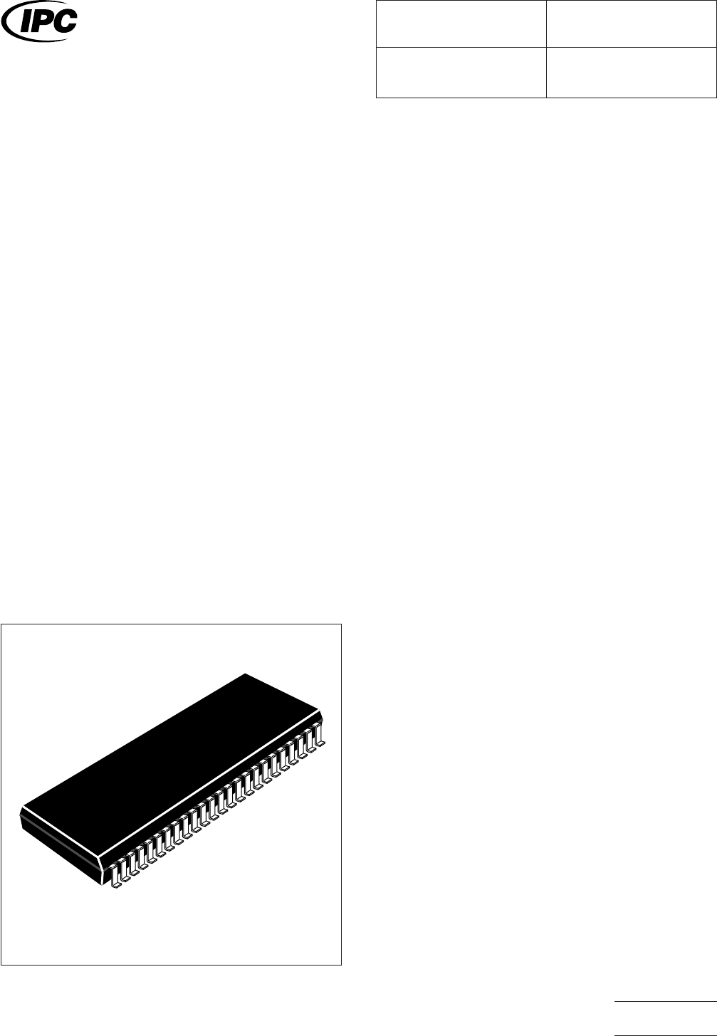
3.1 Basic Construction
See Figure 1. Basic construction
consists of a plastic body and metallic leads.
3.1.1 Termination Materials
Leads should be solder-
coated with a tin/lead alloy. The solder should contain
between 58 to 68% tin. Solder may be applied to the termi-
nation by hot dipping or by plating from solution. Plated sol-
der terminations should be subjected to a post-plating reflow
operation to fuse the solder. The tin/lead finish should be at
least 0.00075 mm [0.0003 in] thick.
3.1.2 Marking
All parts shall be marked with a part number
and ‘‘Pin 1’’ location. ‘‘Pin 1’’ location may be molded into the
plastic body.
3.1.3 Carrier Package Format
Bulk rods, 24 mm tape/
8–12 mm pitch is preferred for best handling. Tube carriers
are also used.
3.1.4 Resistance to Soldering
Parts should be capable of
withstanding ten cycles through a standard reflow system
operating at 215°C. Each cycle shall consist of 60 seconds
exposure at 215°C. Parts must also be capable of withstand-
ing a minimum of 10 seconds immersion in molten solder at
260°C.
IPC-782-9-2-1
Figure 1 SSOIC construction
IPC-SM-782
Surface Mount Design
and Land Pattern Standard
Date
5/96
Section
9.2
Revision
A
Subject
SSOIC
Page1of4
电子技术应用 www.ChinaAET.com
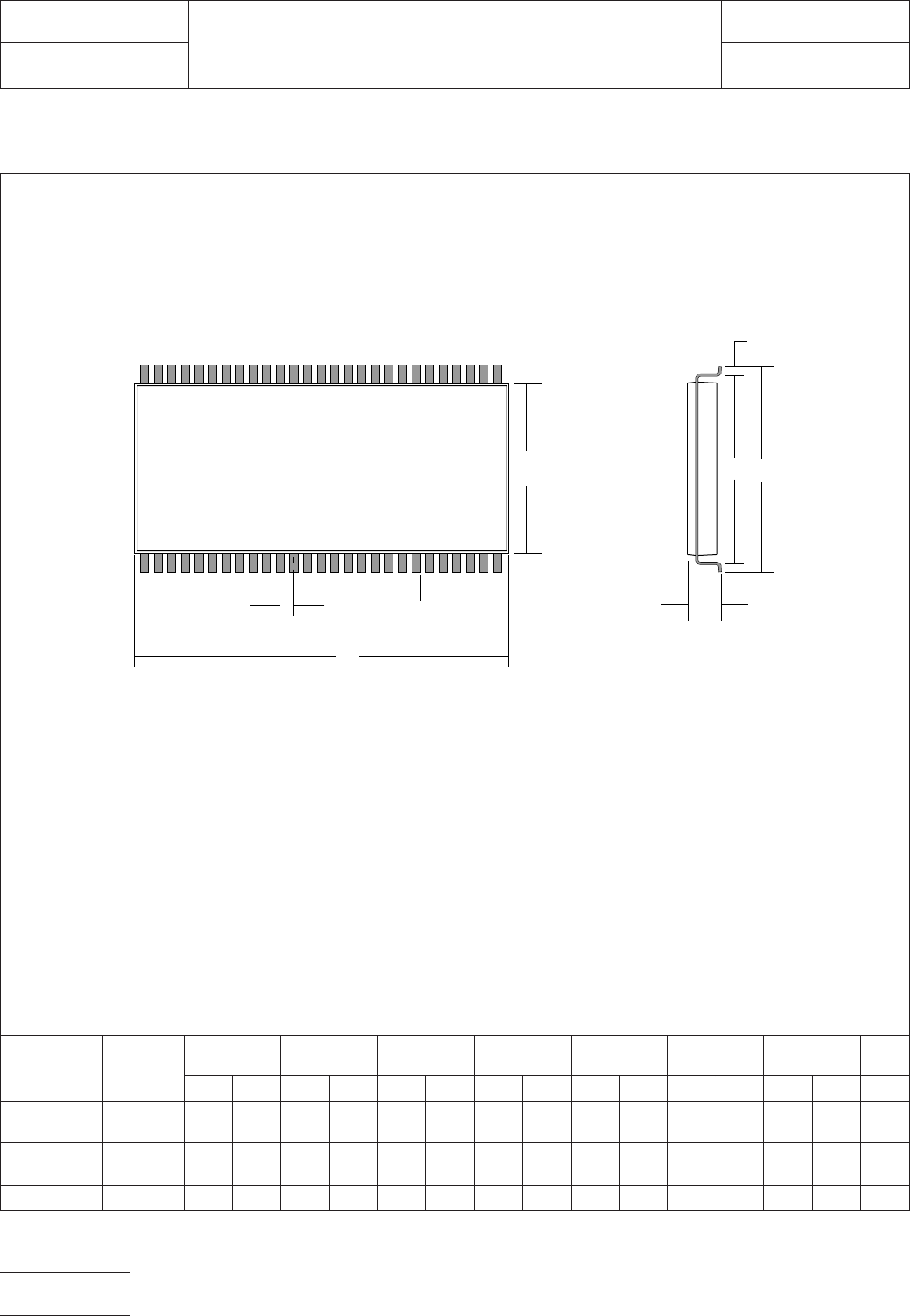
4.0 COMPONENT DIMENSIONS
Figure 2 provides the component dimensions for SSOIC components.
Component
Identifier
JEDEC
Number
L (mm) S (mm) W (mm) A (mm) B (mm) H (mm) T (mm)
P
(mm)
min max min max min max min max min max min max min max basic
SS048 M0118
AA
10.03 10.67 7.99 8.95 0.20 0.30 7.40 7.60 15.75 16.00 2.41 2.20 0.51 1.02 0.635
SS056 M0118
AB
10.03 10.67 7.99 8.95 0.20 0.30 7.40 7.60 18.29 18.54 2.41 2.20 0.51 1.02 0.635
S064 M0117 14.00 14.50 12.40 13.05 0.30 0.45 11.90 12.10 26.17 26.43 1.92 2.00 0.51 0.80 0.800
Figure 2 SSOIC component dimensions
▼
▼
▼
▼
▼
▼
W
B
P
▼
▼
A S
▼
▼
▼
▼
H
▼
T
L
▼
▼
IPC-782-9-2-2
IPC-SM-782
Subject
SSOIC
Date
5/96
Section
9.2
Revision
A
Page2of4
电子技术应用 www.ChinaAET.com
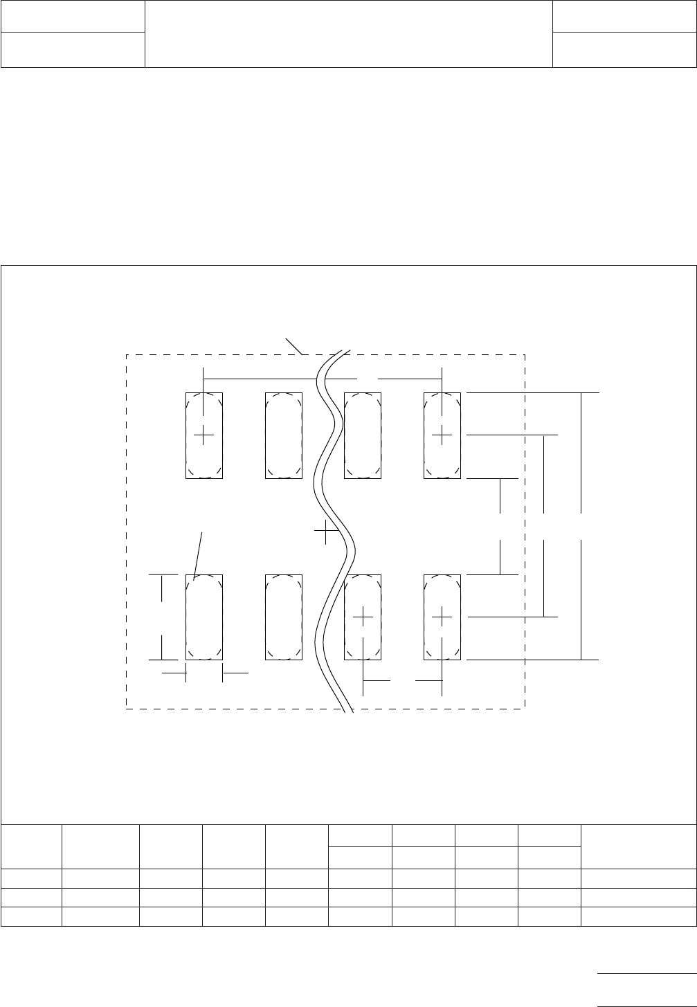
5.0 LAND PATTERN DIMENSIONS
Figure 3 provides the land pattern dimensions for SSOIC
components. These numbers represent industry consensus
on the best dimensions based on empirical knowledge of fab-
ricated land patterns.
In the table, the dimensions shown are at maximum material
condition (MMC). The least material condition (LMC) should
not exceed the fabrication (F) allowance shown on page 4.
The LMC and the MMC provide the limits for each dimension.
The dotted line in Figure 3 shows the grid placement court-
yard which is the area required to place land patterns and
their respective components in adjacent proximity without
interference or shorting. Numbers in the table represent the
number of grid elements (each element is 0.5 by 0.5 mm) in
accordance with the international grid detailed in IEC publica-
tion 97.
RLP No.
Component
Identifier Z (mm) G (mm) X (mm)
YCDE
Placement Grid
(No. Grid
Elements)ref (mm) ref (mm) ref (mm) ref (mm)
330A SS048 11.60 7.20 0.40 2.20 9.40 14.61 0.64 24x34
331A SS056 11.60 7.20 0.40 2.20 9.40 17.15 0.64 24x38
332A S064 15.40 11.40 0.50 2.00 13.40 24.80 0.80 32x54
Figure 3 SSOIC land pattern dimensions
▼
D
X
▼
▼
E
▼
▼
GCZ
▼
▼
▼
▼
▼
▼
▼
Full radius typical
Grid placement courtyard
▼
▼
Y
▼
▼
IPC-782-9-2-3
IPC-SM-782
Subject
SSOIC
Date
5/96
Section
9.2
Revision
A
Page3of4
电子技术应用 www.ChinaAET.com