IPC-SM-782A 表面安装设计和焊盘设计标准(带BGA).pdf - 第144页
6.0 TOLERANCE AND SOLDER JOINT ANALYSIS Figure 4 provides the solder joint minimums for toe, heel, and side fillets, as discussed in Section 3.3. The tolerances are addressed in a statistical mode, and assume even distri…
RLP No.
Component
Identifier
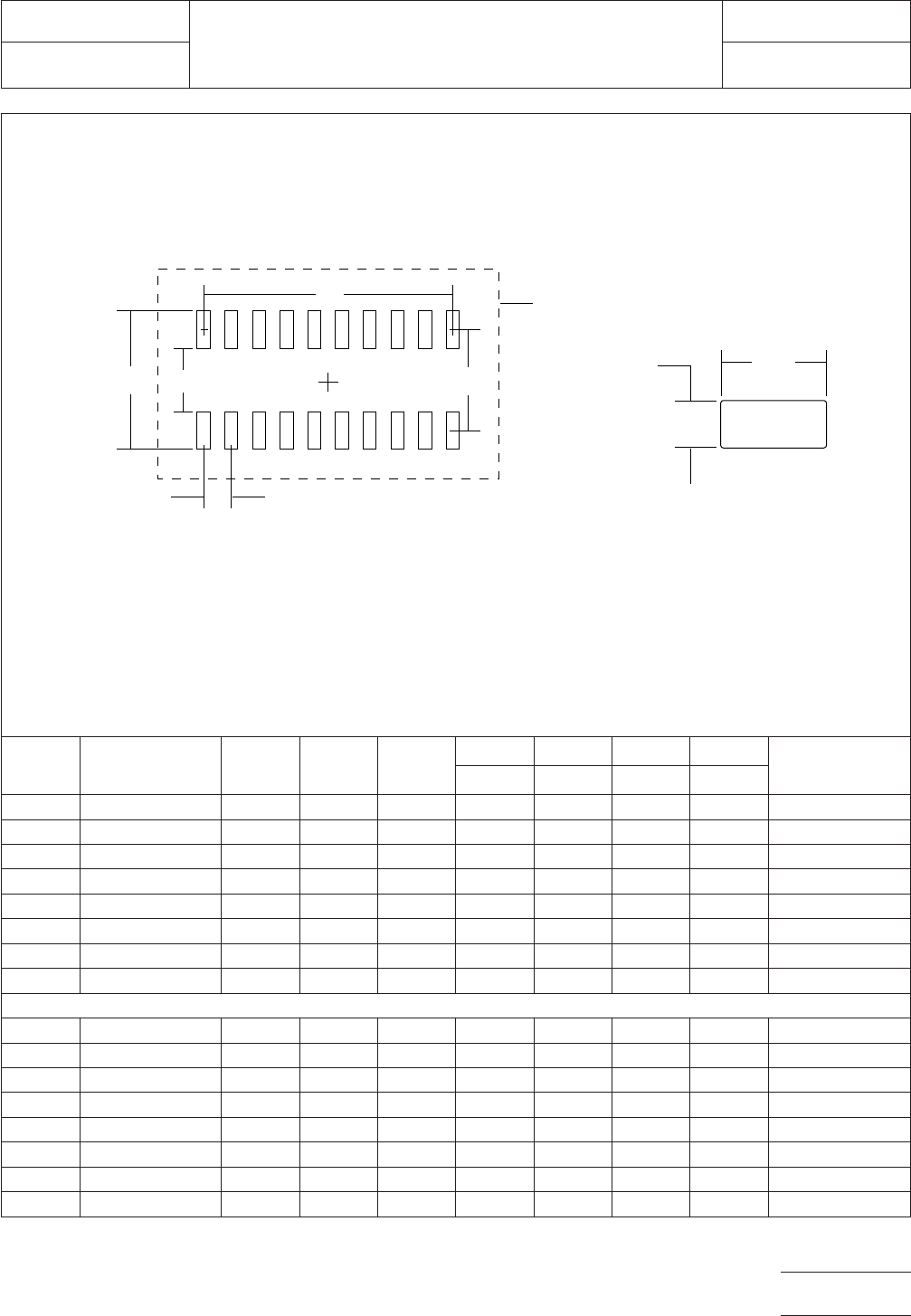
(Pin Count) Z (mm) G (mm) X (mm)
Y (mm) C (mm) D (mm) E (mm)
Placement Grid
(No. Grid
Elements)
ref ref basic basic
500A SOJ 14/400 11.80 7.40 0.60 2.20 9.60 7.62 1.27 26x22
501A SOJ 16/400 11.80 7.40 0.60 2.20 9.60 8.89 1.27 26x24
502A SOJ 18/400 11.80 7.40 0.60 2.20 9.60 10.16 1.27 26x26
503A SOJ 20/400 11.80 7.40 0.60 2.20 9.60 11.43 1.27 26x28
504A SOJ 22/400 11.80 7.40 0.60 2.20 9.60 12.70 1.27 26x32
505A SOJ 24/400 11.80 7.40 0.60 2.20 9.60 13.97 1.27 26x34
506A SOJ 26/400 11.80 7.40 0.60 2.20 9.60 15.24 1.27 26x36
507A SOJ 28/400 11.80 7.40 0.60 2.20 9.60 16.51 1.27 26x38
510A SOJ 14/450 13.20 8.80 0.60 2.20 11.00 7.62 1.27 28x22
511A SOJ 16/450 13.20 8.80 0.60 2.20 11.00 8.89 1.27 28x24
512A SOJ 18/450 13.20 8.80 0.60 2.20 11.00 10.16 1.27 28x26
513A SOJ 20/450 13.20 8.80 0.60 2.20 11.00 11.43 1.27 28x28
514A SOJ 22/450 13.20 8.80 0.60 2.20 11.00 12.70 1.27 28x32
515A SOJ 24/450 13.20 8.80 0.60 2.20 11.00 13.97 1.27 28x34
516A SOJ 26/450 13.20 8.80 0.60 2.20 11.00 15.24 1.27 28x36
517A SOJ 28/450 13.20 8.80 0.60 2.20 11.00 16.51 1.27 28x38
Figure 3b SOJ land pattern dimensions
D
C
▼
▼
▼
▼
GZ
▼
▼
E
▼
▼
▼
▼
Y
X
▼
▼
▼
▼
▼
Grid
Placement
Courtyard
IPC-782-10-1-3B
IPC-SM-782
Subject
SOJ
Date
5/96
Section
10.1
Revision
A
Page5of6
电子技术应用 www.ChinaAET.com
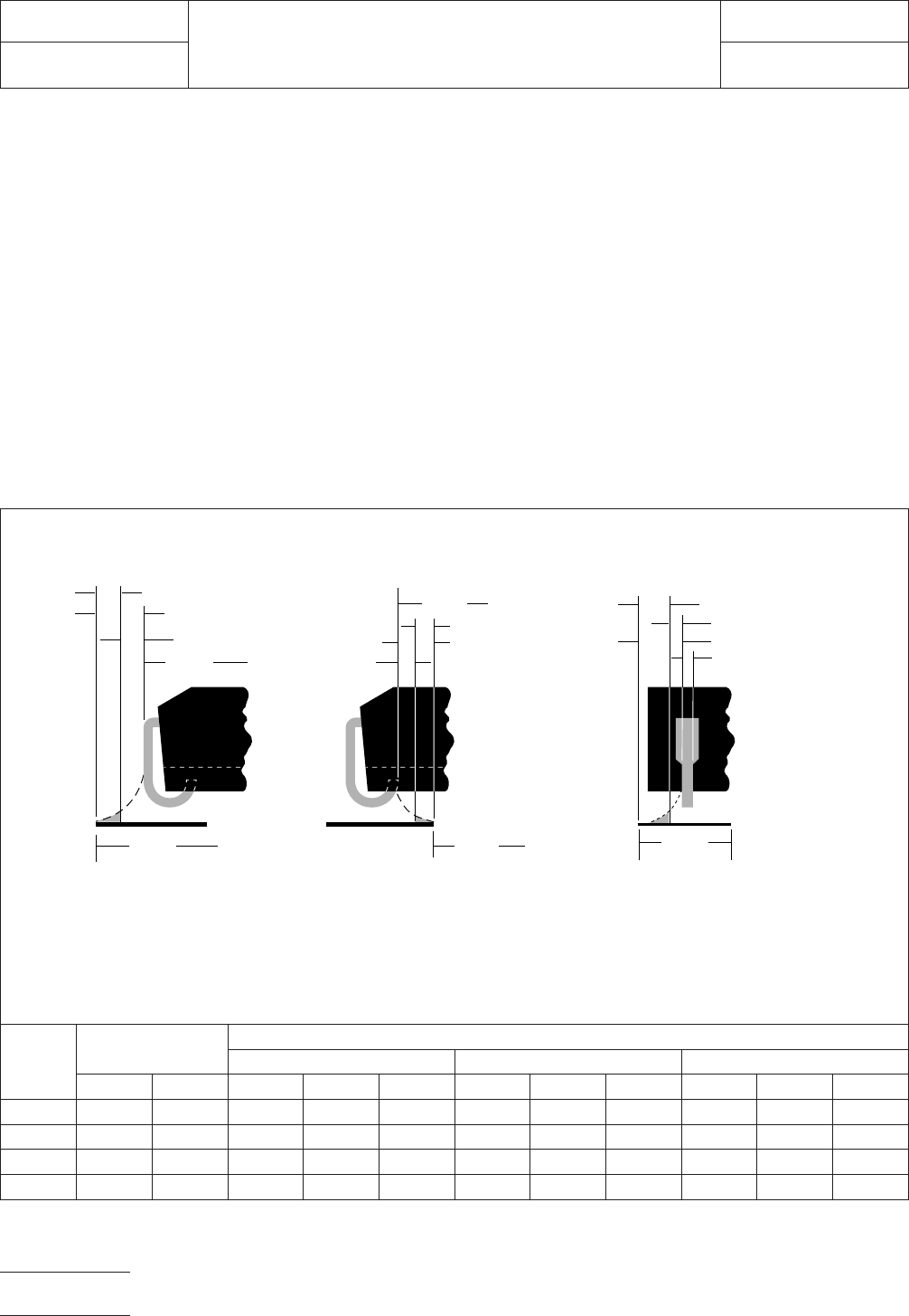
6.0 TOLERANCE AND SOLDER JOINT ANALYSIS
Figure 4 provides the solder joint minimums for toe, heel, and
side fillets, as discussed in Section 3.3. The tolerances are
addressed in a statistical mode, and assume even distribution
of the tolerances for component, fabrication, and placement
accuracy.
Figure 4 provides the solder joint minimums for toe, heel, and
side fillets, as discussed in Section 3.3. The tolerances are
addressed in a statistical mode, and assume even distribution
of the tolerances for component, fabrication, and placement
accuracy.
Individual tolerances for fabrication (‘‘F’’) and component
placement equipment accuracy (‘‘P’’) are assumed to be as
given in the table. These numbers may be modified based on
user equipment capability or fabrication criteria. Component
tolerance ranges (C
L
,C
S
, and C
W
) are derived by subtracting
minimum from maximum dimensions given in Figure 2. The
user may also modify these numbers, based on experience
with their suppliers. Modification of tolerances may result in
alternate land patterns (patterns with dimensions other than
the IPC registered land pattern dimensions).
The dimensions for minimum solder fillets at the toe, heel, or
side (J
T
,J
H
,J
S
) have been determined based on industry
empirical knowledge and reliability testing. Solder joint
strength is greatly determined by solder volume. An observ-
able solder fillet is necessary for evidence of proper wetting.
Thus, the values in the table usually provide for a positive sol-
der fillet. Nevertheless, the user may increase or decrease the
minimum value based on process capability.
RLP No.
Tolerance
Assumptions (mm)
Solder Joint
Heel (mm) Toe (mm) Side (mm)
FPC
S
J
H
min J
H
max C
L
J
T
min J
T
max C
W
J
S
min J
S
max
480-487A 0.10 0.10 0.38 0.31 0.51 0.68 -0.32 0.03 0.13 -0.01 0.11
490-497A 0.10 0.10 0.38 0.27 0.48 0.68 -0.28 0.07 0.13 -0.01 0.11
500-507A 0.10 0.10 0.38 0.24 0.44 0.68 -0.27 0.10 0.13 -0.01 0.11
510-517A 0.10 0.10 0.38 0.30 0.51 0.68 -0.31 0.04 0.13 -0.01 0.11
Figure 4 Tolerance and solder joint analysis
Zmax = Lmin + 2J
T
min + T
T
Where:
J
T
min = Minimum toe fillet
T
T
= Combined tolerances
at toe fillet
Gmin = Smax - 2J
H
min - T
H
Where:
J
H
min = Minimum heel fillet
T
H
= Combined tolerances
at heel fillet
Xmax
Xmax = Wmin + 2J
S
min + T
S
Where:
J
S
min = Minimum side fillet
T
S
= Combined tolerances
at side fillet
▼
▼
Toe Fillet
1
/2 T
S
Heel Fillet Side Fillet
J
S
max
▼
▼
▼
▼
▼
▼
▼
J
S
min
Lmin
▼
▼
Zmax
▼
▼
1
/2 T
T
J
T
min
Smax
J
H
min
1
/2 T
H
▼
▼
▼
▼
▼
▼
▼
▼
J
T
max
J
H
max
▼
▼
▼
▼
▼
▼
▼
▼
▼
▼
▼
Gmin
▼
Wmin
▼
IPC-782-10-1-4
IPC-SM-782
Subject
SOJ
Date
5/96
Section
10.1
Revision
A
Page6of6
电子技术应用 www.ChinaAET.com
1.0 INTRODUCTION
This section covers land patterns for components with gull-
wing leads on four sides. Each subsection contains informa-
tion in accordance with the following format:
1.0 Scope
2.0 Applicable Documents
3.0 General Component Description (Figure 1)
4.0 Component Dimensions (Figure 2)
5.0 Land Pattern Dimensions (Figure 3)
6.0 Tolerance and Solder Joint Analysis (Figure 4)
The following is the table of contents for this section:
2.0 APPLICABLE DOCUMENTS
The following documents, of the issue in effect on the revision
date of this section, form a part of this specification to the
extent specified herein.
2.1 Electronic Industries Association (EIA)
1
EIA-481-A
Taping of Surface Mount Components for Auto-
matic Placement
EIA-481-3
32 mm, 44 mm, and 56 mm Embossed Carrier
Taping of Surface Mount Components for Automated Han-
dling
JEDEC Publication 95
Registered and Standard Outlines for
Solid State and Related Products:
MO 108, issue ‘‘A,’’ dated 10/90
MO 112, issue ‘‘A,’’ dated 8/90
MO 136, issue ‘‘A,’’ dated 8/92, now MS-026
MO 143, issue ‘‘A,’’ dated 3/93, now MS-029
2.2 Electronic Industries Association of Japan (EIAJ)
EIAJ-ED-7404
General Rules for the Preparation of Outline
Drawings of Integrated Circuits
2.3 International Electrotechnical Commission (IEC)
2
IEC 97
Grid Elements
3.0 General Information
3.1 General Component Description
The four-sided gull
wing family is characterized by gull wing leads on four sides of
a square or rectangular package. The family includes both
molded plastic and ceramic case styles. The acronyms PQFP,
Plastic Quad Flat Pack and CQFP, Ceramic Quad Flat Pack,
are also used to describe the family.
There are several lead pitches within the family from 1.0 mm
to 0.30 mm. High lead-count packages are available in this
family that accommodate complex, high lead-count chips.
3.2 Marking
The PFQP and CQFP families of parts are
generally marked with manufacturers part numbers, manufac-
turers name or symbol, and a pin 1 indicator. Some parts may
have a pin 1 feature in the case shape instead of pin 1 mark-
ing. Additional markings may include date code/
manufacturing lot and/or manufacturing location.
3.3 Carrier Package Format
Components may be pro-
vided in tube but packaging tray carriers are preferred for best
handling and high volume applications. Bulk packaging is not
acceptable because of lead coplanarity required for place-
ment and soldering.
3.3 Process Considerations
PQFP and CQFP packages
are normally processed by solder reflow operations.
High lead-count fine pitch parts may require special process-
ing outside the normal pick/place and reflow manufacturing
operations.
Separate pick/place, excise, and reflow processes are some-
times used as an alternate to normal SMT processes.
1. Application for copies should be addressed to Global Engi-
neering Documents, 1990 M St. N.W., Washington, DC
20036.
2. Application for copies should be addressed to IEC, 3 rue
de Varembe, PO Box 131 - 1211 Geneva 20, Switzerland
IPC-SM-782
Surface Mount Design
and Land Pattern Standard
Date
8/93
Section
11.0
Revision Subject
Components with
Gullwing Leads on Four
Sides
Page1of2
电子技术应用 www.ChinaAET.com