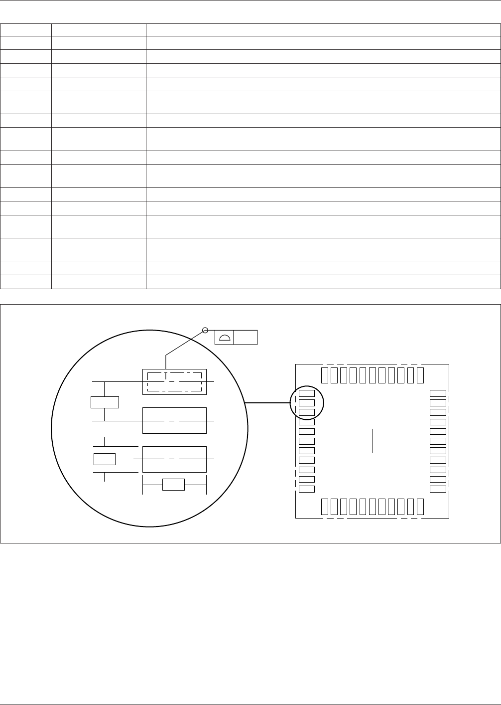
IPC-SM-782A 表面安装设计和焊盘设计标准(带BGA).pdf - 第19页
the length of the capacitor . Figure 3–4b shows the compo- nent length at its minimum size in the converted dimen- sions of the new system using profile tolerancing. Figure 3–4c shows the land pattern at its maximum size.…
Profile tolerances are unilateral, and are described to reflect
the best condition for solder joint formation usually at
minimum component size. As the profile tolerance moves
in this unilateral direction toward maximum component
size, the opportunity for a robust solder joint decreases.
The concept for component dimension evaluations is based
on evaluating the surfaces of the component termination
and component lead that are involved in the formation of
the acceptable solder joint. Component manufacturers usu-
ally provide dimensions for their parts with a nominal size
and then put a tolerance on that nominal dimension. Inor-
der to facilitate the dimensioning system, these dimensions
and their associated tolerances are converted to minimum
and maximum size.
As an example, capacitor C1206 has a manufactured nomi-
nal dimension for its length (L) of 3.2 mm. The tolerance
described by the manufacturer is
˜
0.2 mm. Thus, the mini-
mum dimension of ‘‘L’’ is 3.0 mm with a unilateral toler-
ance of 0.4 mm, resulting in its maximum dimension being
3.4 mm.
Figure 3–4 shows the characteristics for the C1206. Figure
3–4a shows the component manufacturers dimensions for
IPC-782-3-2
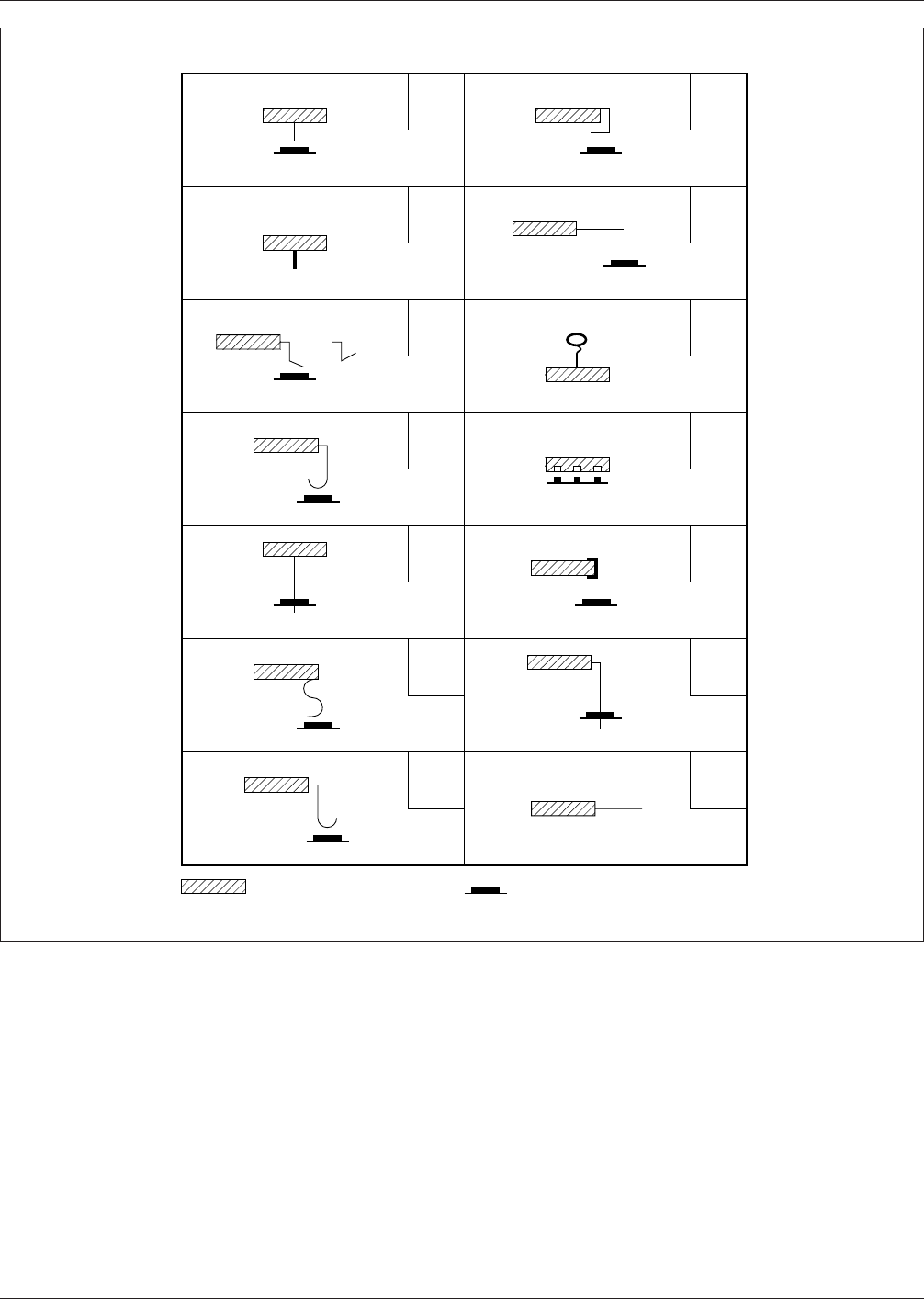
Figure 3–2 Lead-form (or terminal-shape) examples
B
D
G
J
P
S
U
C
F
H
N
R
T
W
BUTT "C" BEND
SOLDER LUG FLAT
GULL WING HIGH-CURRENT CABLE
"J" BEND NO LEAD
PIN/PEG WRAPAROUND
"S" BEND THROUGH-HOLE
"J" INVERTED WIRE
BODY OF PACKAGE LAND STRUCTURE
IPC-SM-782A December 1999
10
电子技术应用 www.ChinaAET.com
the length of the capacitor. Figure 3–4b shows the compo-
nent length at its minimum size in the converted dimen-
sions of the new system using profile tolerancing. Figure
3–4c shows the land pattern at its maximum size. These
conditions provide for an optimum toe fillet. For optimum
heel fillet the component basic dimensions are at the maxi-
mum and the land pattern is at its minimum.
Similar concepts are applied to leaded surface mount parts.
The critical dimensional characteristics identified are those
that relate to the formation of the toe and heel solder fillet.
For components with gull wing leads the basic dimensions
apply across the outer extremities of the part for toe solder
fillet formation; and within the inside of the formed radius
of opposing leads for heel solder fillet formation.
The outer dimensions of leaded or even leadless chip car-
riers are usually easy to determine since these are readily
available from the component manufacturer. The inner
(heel-to-heel) dimensions are not provided in industry stan-
dards or manufacturer’s specifications, and are more diffi-
cult to determine, not only because of the form of the lead,
Table 3–3 Lead-Form (or Terminal-Shape) Suffixes
Code Form/Shape Description (see Figure A2)
B Butt A noncompliant lead intended for attachment perpendicular to the land structure.
C ‘‘C’’ bend A ‘‘C’’ shaped noncompliant lead bent down and under the body of the package.
D Solder lug A lug terminal on the package
F Flat A noncompliant, nonformed flat lead that extends away form the body of the package.
G Gull wing A compliant lead bent down from the body of the package with a foot at the end pointing
away from the package.
H High-current cable A lug terminal at the end of a flexible lead.
J ‘‘J’’ bend A ‘‘J’’ shaped compliant or noncompliant lead bent down and back under the body of the
package.
N No lead Metallized terminal pads located on the body of the package.
P Pin/Peg A tempered lead extending from the body of the package and intended for attachment to a
plated through-hole in the land structure.
R Wraparound A metallized noncompliant terminal wrapped around the package body.
S ‘‘S’’ bend An ‘‘S’’ shaped compliant lead bent under the body of the package.
T Through-hole A terminal with flat or V-shaped cross section intended for attachment to a plated
through-hole in the land structure.
U ‘‘J’’ inverted A ‘‘J’’ shaped compliant or noncompliant lead bent down form the doby of the package with
the curved end pointing away from the package.
W Wire An untempered wire lead extending from the body of the package.
X Other A lead form or terminal shape other than those defined.
IPC-782-3-3
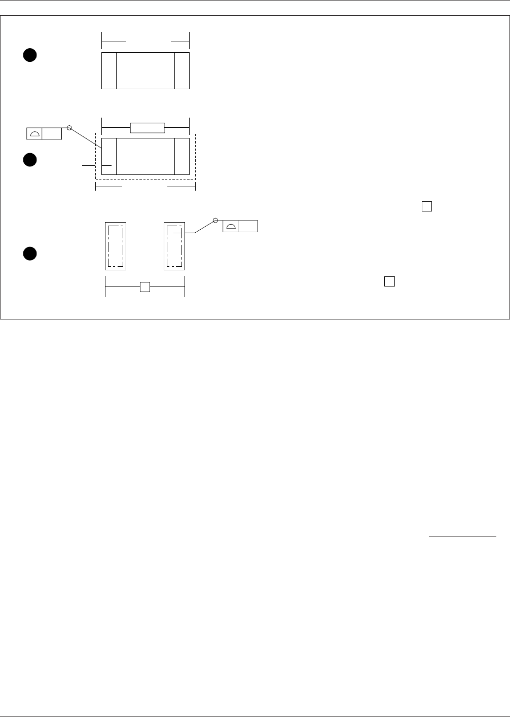
Figure 3–3 Profile tolerancing examples
0.7
1.27
▼
▼
▼
▼
▼
2.5
MMC
▼
▼
▼
0.1
MMC
"
N
"
Places
December 1999 IPC-SM-782A
11
电子技术应用 www.ChinaAET.com
termination, or castellation; but also because the inner
dimensions must be derived by subtracting the sum of the
dimensions of the leads (with all their inherent tolerances)
from the overall dimensions of the part.
Figure 3–5a shows the concept for the manufacturers
dimensions and tolerances for a gull-wing SOIC. Figure
3–5b shows the converted dimensions to be considered in
the overall mounting system requirements. Figure 3–5c
shows the land pattern dimensions. The basic dimensions
define the minimum length as measured across the two
outer extremities. Tolerances increase this dimension to the
maximum width, reducing toe fillet opportunity. The inner
dimensions between heel fillets on opposing sides are the
most important. Inner dimensions are derived by:
a. Establishing the maximum width of the component as
measured from lead termination to lead termination.
(This dimension is shown as ‘‘L,’’ and is provided by
the manufacturer).
b. Establishing the minimum amount of the lead length as
measured across the ‘‘footprint’’ (from heel to toe for
gull-wing leads). (This dimension is ‘‘T,’’ and is pro-
vided by the manufacturer).
c. Subtracting twice the minimum lead length of (b) from
the maximum overall component length of (a) to arrive
at the maximum length inside the leads across the length
of the component (the inner dimension between oppos-
ing heel fillets). Including the tolerances on dimensions
(a) and (b) will yield the minimum dimension between
opposing heels. This signifies worst case tolerance
analysis.
d. Three sets of tolerances are involved in the analysis
described in (c.); tolerances on the overall component,
plus the tolerances for the lead on each end. Since not
all three tolerances are considered at their worse case, a
recommended method for determining the statistical
impact is to summarize the squares of the tolerances and
take the square-root of their sum as the rms (root-mean-
square) tolerance difference.
For example:
RMS tolerance accumulation =
√
(L
tol
)
2
+ 2(T
tol
)
2
Where:
L
tol
=L
max
–L
min
T
tol
=T
max
–T
min
As an example, the SOIC with 16 leads has the follow-
ing limits for the ‘‘L’’ (component length) and ‘‘T’’ (ter-
minal length) dimensions:
L
min
= 5.8 mm, L
max
= 6.2 mm
L
tol
=L
max
–L
min
= 6.2 – 5.8 = 0.4 mm
T
min
= 0.4 mm, T
max
= 1.27 mm
T
tol
=T
max
–T
min
= 1.27 – 0.4 = 0.87 mm
IPC-782-3-4
Figure 3–4 Example of C1206 capacitor dimensioning for optimum solder fillet conditions
3.2 ± 0.2
mm
▼
▼
▼
▼
3.0 LMC
▼
0.2
▼
▼
Maximum
component size
▼
▼
Z
MMC
▼
▼
▼
▼
0.05
Manufacturers dimensions
and tolerances
(maximum length of part is 3.4
mm).
Part shown with length at
"least material condition", and
profile tolerance to indicate
maximum range of
component length at 3.4
mm.
Land pattern with dimension Z at
"maximum material condition". Profile
tolerance of part (0.2 X 2), plus profile
tolerance of land pattern (0.05 X 2) plus
placement accuracy (0.1 diameter of true
position) are considered in determining the
proper dimension for Z , plus the desired
toe fillet.
A
B
C
IPC-SM-782A December 1999
12
电子技术应用 www.ChinaAET.com