IPC-SM-782A 表面安装设计和焊盘设计标准(带BGA).pdf - 第16页
a. All dimensions are basic (nominal) b. Limits of size control form as well as size. c. Perfect form is required at maximum dimensions. d. Datum references and position tolerances apply at maxi- mum dimensions, and are …

slot or edge, used exclusively to position the board or panel
or to mount components accurately. (See Fiducial)
*Via – A plated-through hole used as a through connection,
but in which there is no intention to insert a component
lead or other reinforcing material.
Blind via – A via that is connected to either the primary
side or secondary side and one or more internal layers of a
multilayer packaging and interconnecting structure, but not
to both sides.
Buried via – A via that is connected to neither the primary
side nor the secondary side of a multilayer packaging and
interconnecting structure, i.e., it connects only between
inner layers.
Tented via – A blind or through-hole via that has the
exposed surface of the primary or secondary or both sides
of a packaging and interconnecting structure fully covered
by a masking material, such as a dry film polymer coating
(solder mask), preimpregnated glass cloth (prepreg), etc., in
order to prevent hole access by process solutions, solder, or
contamination.
3.2 Component Acronyms
In an attempt to standardize
on component characteristics the Joint Electronic Device
Engineering Council (JEDEC) of the Electronic Industries
Association (EIA) has developed a set of recommended
acronyms that can be used to describe the shape, material,
lead position, package style, lead form and lead count.
These details are defined in JEDEC Publication JESD1C
and have been circulated and approved as an international
document published by the International Electrotechnical
Commission (IEC) as IEC Publication 30. These concepts
are supported and adopted in this land pattern document to
facilitate communication between design, component
manufacturer, board manufacturer, quality assurance etc.
Some of the information from the JEDEC publication is
presented to assist the reader. The acronym systems is
divided into six parts. They are:
• SHAPE – A single-letter prefix that identifies the
mechanical package profile (round, rectangular, square,
etc.)
• MATERIAL – A single-letter prefix that identifies the
predominant package body material (glass, metal,
plastic, etc.)
• POSITION – A single-letter prefix that identifies termi-
nal or lead position related to the package profile (see
3.2.1)
• PACKAGE – A double-letter designation that identifies
the package-outline style (see 3.2.2)
• FORM – A single letter suffix that identifies the terminal
or lead form (see 3.2.3)
• COUNT – A one, two, or three-digit suffix that identifies
the number of leads or terminations (12, 84, 160, etc.)
The minimum acronym consists of the position, package,
form and count identifiers. Shape and material prefixes are
optional acronym designations. As an example the designa-
tion R-PDIP-T14 describes a rectangular part (R), made of
plastic (P), with dual terminals or leads (D), coming from
an in-line package style (IP) with through-hole leads (T)
and a lead count of 14.
3.2.1 Position Designation
The single-letter prefix for
terminal position shall be identified in accordance with
Table 3–1. The position definition ‘‘terminal’’ applies to
either lead or leadless. The descriptions assume that the
seating plane is the bottom of the package. Reference to
package shape does not take into account flanges, notches
or irregularities.
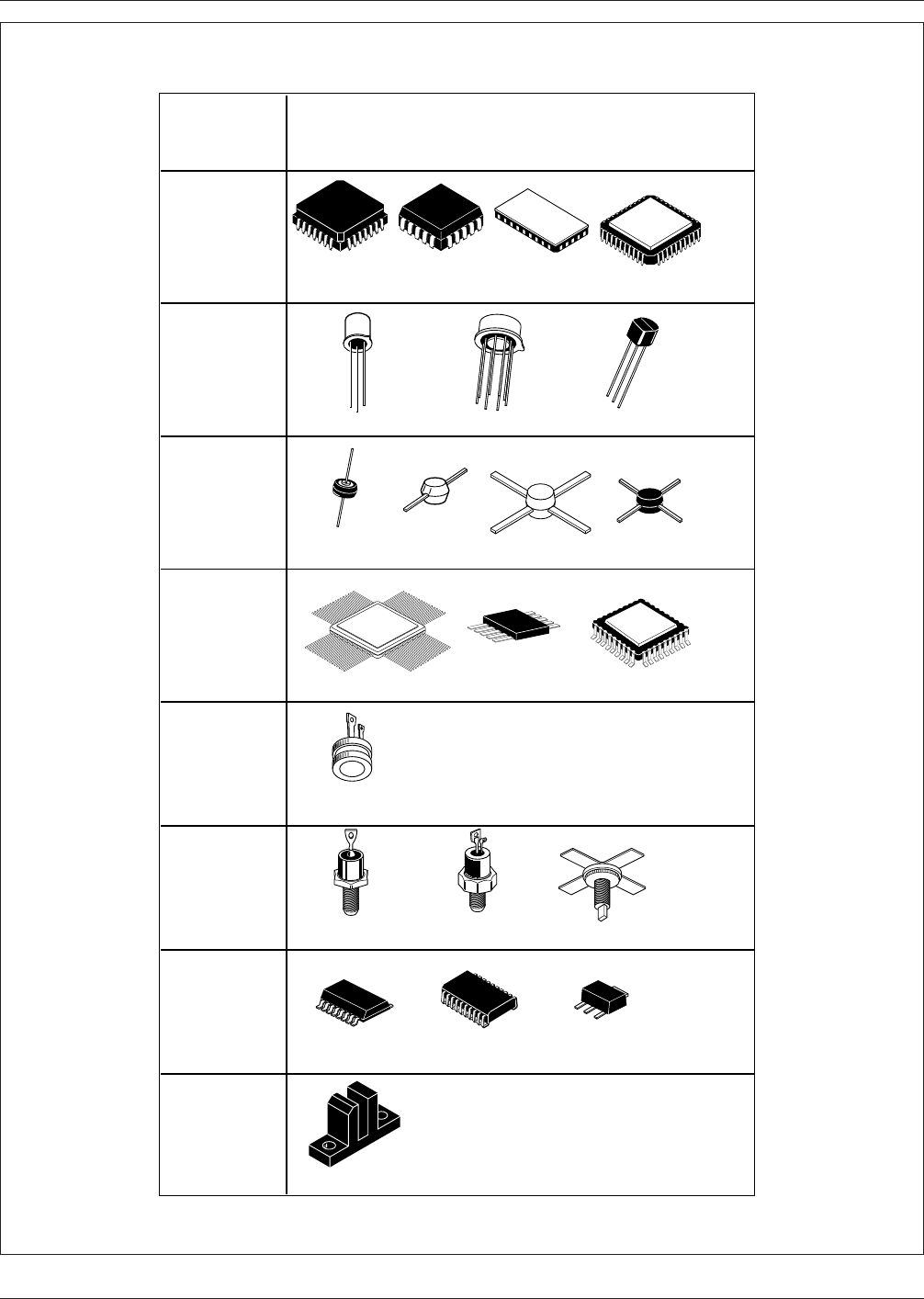
3.2.2 Package-Outline Style Designators
The package
double-letter designator shall be in accordance with Table
3–2. Figure 3–1 provides some examples of the compul-
sory package outline style acronyms.
3.2.3 Form Designation
The single-letter suffix that
defines the terminal form (termination or lead) configura-
tion shall be in accordance with Table 3–3. Figure 3–2
shows a few diagrams of various package lead configura-
tions.
3.3 Dimensioning Systems
There are many methods of
dimensioning and tolerancing mechanical parts, all of
which are defined in ANSI Y14.5. All the methods work,
but it must be recognized that some methods work better
than others and some methods cost less to inspect or evalu-
ate product than others. This section describes a set of
dimensional criteria for components, land patterns, posi-
tional accuracy of the component placement capability and
the opportunity to create a certain size solder joint com-
mensurate with reliability or product performance analysis.
Sections 8.0 through section 13.0 define the specific details
of various electronic and electromechanical component
families. Each section describes the mounting dimensions
for the component and the specific land pattern that may be
used to surface mount that particular component or compo-
nent family. In addition, an analysis is made to establish
the land pattern sizes that take into account the accuracy of
the placement operation and requirements for the solder
joint.
Profile tolerances are used in the dimensioning system to
control the size range between maximum and minimum
component/lead dimensions without ambiguity. The profile
tolerance is intended to control both size and position of
the land. Figure 3–3 shows the profile tolerancing method.
The use of the profile dimensioning system requires an
understanding of the concepts detailed in ANSI Y14.5. The
use of a set of requirements are adopted and invoke the
following rules, unless otherwise modified:
December 1999 IPC-SM-782A
7
电子技术应用 www.ChinaAET.com
a. All dimensions are basic (nominal)
b. Limits of size control form as well as size.
c. Perfect form is required at maximum dimensions.
d. Datum references and position tolerances apply at maxi-
mum dimensions, and are dependent on feature size.
e. Position dimensions originate from maximum dimen-
sions.
f. Tolerances and their datum references other than size
and position apply regardless of feature size (RFS).
g. Interpretations are per ANSI Y14.5.
The dimensioning concepts used for this system of analy-
sis consider the assembly/attachment requirements as their
major goal. Specification (data) sheets for components or
dimensions for land patterns on boards may use different
dimensioning concepts, however, the goal is to combine all
concepts into a single system. Users are encouraged to
establish the appropriate relationship between their dimen-
sioning system(s) and the profile dimensioning system and
analysis concepts described herein to allow for ease of tai-
loring these concepts for robust process performance. As
an example, if the tolerance used for positioning is larger
than the machine tolerance used in production, a single
dimensional change in a ‘‘spread sheet’’ program could
modify the land pattern dimensions shown in sections 8.0
through 13.0 in order to optimize the process for a given
facility.
3.3.1 Component Tolerancing
The component manu-
facturers and the Electronic Industries Association (EIA)
are responsible for the dimensioning and tolerancing of
electronic components. Their concepts have been converted
to a functional equivalent using the profile tolerancing
method with all components shown with their basic dimen-
sions as limit dimensions (maximum or minimum size).
Table 3–1 Terminal Position Prefixes
Code Name Position (see notes 1 and 2)
A Axial Terminal extend from both ends in the direction of the major axis of a cylindrical or elliptical
package.
B Bottom Terminals beneath the seating plan of the package.
D Dual Terminals on opposite sides of a square or rectangular package or located in two parallel rows.
E End Terminals are package endcaps having circular or elliptical cross section.
L Lateral Terminals are on the four sides of a square or rectangular package. The preferred name is
‘‘Quad,’’ code Q.
P Perpendicular Pins are perpendicular to seating plan on a square or rectangular package. Restrict to PGA
family.
Q Quad Terminals are on the four sides of a square or rectangular package or located in four parallel
rows.
R Radial Terminals extend radially from the periphery of a cylindrical or spherical package
S Single Terminals are on one surface of a square or rectangular package in a single row.
T Triple Terminals are on three sides of a square or rectangular package.
U Upper Terminals are perpendicular to and opposite the seating plane, and are on one surface of a
package.
X Other Terminal positions other than those described.
Z Zig-zag Terminals are on one surface of a square or rectangular package arranged in a staggered
configuration. Restrict to ZIP family.
NOTE 1: These descriptions assume the seating plane is the bottom of the package.
NOTE 2: Reference to package shape does not take into account flanges, notches, or irregularities.
Table 3–2 Package-Outline-Style Codes
Code Outline Style
CC Chip-carrier package
CY Cylinder or can package
DB Disc-button package
FM Flange-mount package
FO Fiber-optic-device package
FP Flatpack package
GA Grid-array package
IL In-line package. The preferred designator is IP
IP In-line package or inserted package. Restrict to
DIP/SIP/ZIP.
LF Long-form horizontal package.
MA Microelectronic assembly.
MW Microwave package
PF Press-fit package
PM Post-/stud-mount package
SO Small-outline package
SS Special-shape package
UC Uncased chip
XA-XZ Nondefiend family; vendor or user option.
IPC-SM-782A December 1999
8
电子技术应用 www.ChinaAET.com
IPC-782-3-1
Figure 3–1 Examples of typical package styles and package descriptive designators
Examples
Package
Outline
Style
and Code
CC
Chip Carrier
PQCC PQCC
(PLCC)
PQCC
(CLCC)
PQCC
(CLCC)
CY
Cylinder
DB
Disk Button
MBCY MBCY
CQFP
LRDB GRDB PRDB
PBCY
PF
Press Fit
PM
Post/Stud
Mount
SO
Small
Outline
SS
Special
Shape
MUPF
MUPM MUPM CRPM
PDSS
PDSO PDSO PSSO
FP
Flatpack
PADB
CDFP PQFP
December 1999 IPC-SM-782A
9
电子技术应用 www.ChinaAET.com