IPC-SM-782A 表面安装设计和焊盘设计标准(带BGA).pdf - 第33页
soldermask should get onto the optical target, some vision alignment systems may be rendered useless due to insuf f i- cient contrast at the target site. The internal layer background for all fiducials must be the same. T…
3.6.1.9 Fiducial Mark Design Specifications
The Sur-
face Mount Equipment Manufacturers Association
(SMEMA) has standardized on the design rules for fidu-
cials. These rules are supported by the IPC and consist of:
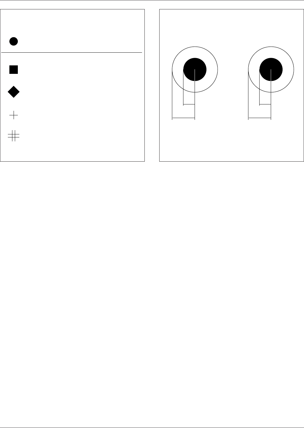
A. Shape
The optimum fiducial mark is a solid filled circle. See
Figure 3–13.
B. Size
The minimum diameter of the fiducial mark is 1 mm
[0.040 in]. The maximum diameter of the mark is 3
mm [0.120 in]. Fiducial marks should not vary in size
on the same PB more than 25 microns [0.001 in].
C. Clearance
A clear area devoid of any other circuit features or
markings shall exist around the fiducial mark. The size
of the clear area shall be equal to the radius of the
mark. A preferred clearance around the mark is equal
to the mark diameter. (See Figure 3–14)
D. Material
The fiducial may be bare copper, bare copper protected
by a clear anti oxidation coating, nickel or tin plated,
or solder coated (hot air leveled).
The preferred thickness of plating or solder coating is
0.005 mm to 0.010 mm [0.0002 to 0.0004 in]. Solder
coating should never exceed 0.025 mm [0.001 in].
If solder mask is used, it should not cover the fiducial
or the clearance area. It should be noted that oxidation
of a fiducial mark’s surface may degrade its readabil-
ity.
E. Flatness
The flatness of the surface of the fiducial mark should
be within 0.015 mm [0.0006 in].
F. Edge Clearance
The fiducial shall be located no closer to the PB edge
than the sum of 4.75 mm [0.187 in] (SMEMA Standard
Transport Clearance) and the minimum fiducial clear-
ance required.
G. Contrast
Best performance is achieved when a consistent high
contrast is present between the fiducial mark and the
PB base material.
It is good design practice to locate global or panel fiducials
in a three point grid based datum system as shown in Fig-
ure 3–15. The first fiducial is located at the 0,0 location.
The second and third fiducials are located in the X and Y
directions from 0,0 in the positive quadrant. The global
fiducials should be located on the top and bottom layers of
all printed boards that contain Surface Mount as well as
Through Hole components since even Through Hole
assembly systems are beginning to utilize vision alignment
systems.
All Fine Pitch components should have two local fiducials
system designed into the component land pattern to insure
that enough fiducials are available every time the compo-
nent is placed, removed and/or replaced on the board. All
fiducials should have a soldermask opening large enough to
keep the optical target absolutely free of soldermask. If
IPC-782-3-13
Figure 3-13 Fiducial types for vision systems
Solid round dot typically 1.5mm Dia.
Preferred
Solid square typically 2.0mm on a side
Solid diamond typically 2.0mm on a side
Single cross hair typically 2.0mm high
Double cross hair typically 2.0mm high
Other
IPC-782-3-14
Figure 3-14 Fiducial clearance requirements
R
2R
Clearance
R
3R
Clearance
Minimum Preferred
▼
▼
▼
▼
▼
▼
▼
▼
IPC-SM-782A December 1999
24
电子技术应用 www.ChinaAET.com
soldermask should get onto the optical target, some vision
alignment systems may be rendered useless due to insuffi-
cient contrast at the target site.
The internal layer background for all fiducials must be the
same. That is, if solid copper planes are retained under
fiducials in the layer below the surface layer, all fiducials
must have copper retained. If copper is clear under one
fiducial, all must be clear.
3.6.2 Conductors
3.6.2.1 Conductor Width & Clearances
Increased com-
ponent density on SMT designs has mandated the use of
thinner conductor density and clearance between conduc-
tors with increased PB layer counts requiring the use of
more vias to make the necessary connections between the
additional layers. Figure 3–16 shows the effects of SMT
and Fine Pitch Technology (FPT) on printed board geom-
etries.
Conductor width/clearances of 0.15 mm [0.006 in] have
become commonplace today, and have basically replaced
the 0.3 mm [0.012 in] line/ space as a commonly used
geometry (see Figure 3–17). As more fine pitch (including
Tape Automated Bonding) devices are used on printed
boards, the 0.125 mm [0.005 in] geometry may be used in
more SMT boards to reduce layer counts. Figure 3–18
IPC-782-3-15
Figure 3–15 Fiducial locations on a printed circuit board
Locate all fiducials and tooling holes on the appropriate grid.
Locate fiducials on both primary and secondary side of board.
Standard tooling hole diameters: 2.4mm, 2.8mm, 3.2mm
Global fiducials should be 5.0mm Min from board edges.
Global fiducials
0
/
0
Point of origin
Fine
Pitch
Component
▼
▼
▼
Local fiducials
IPC-782-3-16
Figure 3–16 Packaging and geometries
GEOMETRY
PIN COUNTS
PLACEMENT TOLERANCE
CONDUCTORS/CLEARANCE
LANDS
HOLES
ANNULAR RING
8 TO 64
.25mm
.3mm
1.5mm
1.0mm
.25mm
8 TO 124
0.125mm
0.15mm
0.75mm
0.4mm
0.2mm
84 TO 244
0.05mm
0.125mm
0.63mm
0.40mm
0.125mm
2.54mm Pitch 1.25mm Pitch 0.63mm Pitch
December 1999 IPC-SM-782A
25
电子技术应用 www.ChinaAET.com
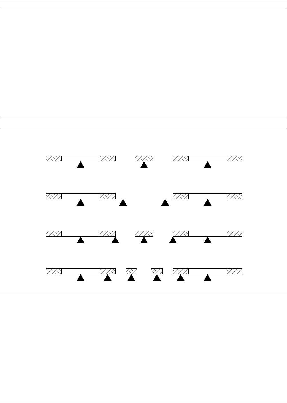
shows a grid routing analysis with vias on 1.0 mm [0.050
in] centers. On the left side are listed the routing grids with
the actual routing channels denoted by solid triangular
points. It can be seen that with SMT geometry of vias
placed on 1.0 mm [0.040 in] centers, there is one routing
channel between lands using a 0.3 mm [0.012 in] grid with
0.15 mm [0.006 in] conductor width/clearances. The bot-
tom routing grid of 0.25 mm [0.010 in] with 0.125 mm
[0.005 in] has two routing channels between vias.
3.6.2.2 Surface Conductors
Wide conductors connect-
ing to a land area can act as a solder thief by drawing sol-
der away from the land and down the conductor. Further-
more, if the conductor goes to a via which is connected to
an inner layer power or ground plane, the wide conductor
may act as a heat sink and draw heat away from the land/
lead area during reflow solder resulting in a cold solder
joint.
A. Narrow the conductor as it enters the land area. Maxi-
mum conductor width should be 0.25 mm [0.010 in]
(see Figure 3–19). The minimum conductor length
should be 0.50 mm [0.020 in]. This neckdown provides
an effective solder restriction, and may eliminate the
IPC-782-3-17
Figure 3–17 Surface mount conductor widths/clearances vs. routing grids
ROUTING GRIDS
.63mm
0.5mm
0.4mm
0.3mm
0.25mm
MANUFACTURING
ALLOWANCE
0.1mm
0.1mm
0.05mm
0.05mm
0.05mm
MINIMUM
CONDUCTORS/CLEARANCE
0.3/0.2mm
0.2/0.2mm
0.2/0.15mm
0.15/0.1mm
0.10/0.10mm
IPC-782-3-18
Figure 3–18 Section view of multilayer board with vias on 1.0 mm [0.040 in] centers
0.5mm SQ Land MIN 0.25mm DRILL
.5mm
GRID
.33mm
GRID
.25mm
GRID
.20mm
GRID
One
Track
Zero
Track
One
Track
Two
Track
.16mm .16mm
.18mm
.18mm
.16mm .16mm
.125mm .125mm
.125mm .125mm.125mm
IPC-SM-782A December 1999
26
电子技术应用 www.ChinaAET.com