IPC-SM-782A 表面安装设计和焊盘设计标准(带BGA).pdf - 第53页
5.0 TESTABILITY 5.1 Testing Considerations 5.1.1 Bare Board Test In testing printed board using through hole technology , the defect rate and the test meth- ods chosen are the principle determiners of overall test cost. …
IPC-782-4-12
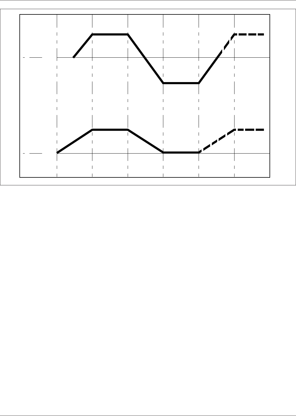
Figure 4–12 Thermal cycle excursion rate
+ 125°
+ 100°
- 65°
400
Cycles
1000
Cycles
0°C
0°C
30
Minutes
30
Minutes
30
Minutes
30
Minutes
30
Minutes
IPC-SM-782A December 1999
44
电子技术应用 www.ChinaAET.com

5.0 TESTABILITY
5.1 Testing Considerations
5.1.1 Bare Board Test
In testing printed board using
through hole technology, the defect rate and the test meth-
ods chosen are the principle determiners of overall test
cost. Real estate considerations (specifically the percentage
of nodes that are available for bed-of-nails probing) are not
a concern, since 100% nodal access practically comes ‘‘for
free’’. In testing surface mount boards, however, real estate
considerations (in addition to defect rates) impact test
costs, since nodal access determines which test methods
are possible and effective.
5.1.2 Loaded Board Test
Given the same test costs,
defect rate can be traded off against real estate. For
example, if the defect rate is relatively high, most boards
will require diagnosis, and the economics of Automatic
Test Equipment (ATE) will demand that full nodal access
be provided for in the board layout. If the defect rate is
low, more time can be spent diagnosing each defect manu-
ally, rather than with ATE, and thus reduce the real estate
impact to less than 100% nodal access. Extremely low
defect levels would theoretically allow 0% nodal access
(no bed of nails test at all), applying only a simple pass/no-
pass test through the edge connector, and throw away fail-
ing assemblies rather than diagnose them.
The major considerations in determining nodal access are:
• Defect rate
• Diagnostic capability
• Real estate impact
—Board area
—Layer count
• Cost impact
Determining the percentage of nodal access to design into
a board layout requires trading off all the issues discussed
previously: defect rate, test development cost, test opera-
tion costs including manual troubleshooting costs, and of
course, impacts on real estate. Short of having no defects
at all, full nodal access remains the most desirable option.
As with Through Hole Technology boards, once the board
is designed (nodal access fixed) and its tests are designed
(test methods fixed), the defect rate becomes the primary
key to reducing test costs. Therefore, defect reporting,
analysis, and correction/prevention are imperative. This
may involve closer supplier relationships to reduce compo-
nent and board level problems, and in-house action to
reduce process-induced problems.
5.2 Nodal Access
In the early stages of product develop-
ment cycles, test philosophies and strategies are often
undefined. This is especially true when a company is mov-
ing from one level of packaging technology to the next
higher level of packaging technology, for example, from
through-hole technology to surface mount technology. Dur-
ing these transition periods, the concurrent engineering
approach is essential for designing nodal access for test-
ability into the product. Concurrent engineering is the prin-
ciple vehicle by which test priorities can and should be
moved up to the beginning of the design cycle and
addressed with a higher priority. In the early stages of a
design, a test philosophy should be clearly defined, then a
strategy for executing the tests can be implemented. An
ideal philosophy to adopt is one that identifies all of the
different test types and the level of test that each type
requires.
There are 2 basic categories of PB tests: The bare board
test, and the loaded board test. The bare board test is per-
formed at the end of the fabrication cycle and checks for
shorts, opens, and net list connectivity. The loaded board
tests occur at the end of the assembly cycle and are consid-
erably more complex. They include: Manufacturing
Defects Analyzer (MDA), in-circuit, functional and combi-
national tests.
The test philosophy should be written to encompass what-
ever combination of tests are necessary for the product.
Then, a simple strategy for implementing the required tests
can be defined prior to beginning the design process. Plan-
ning testability at the beginning of a product development
cycle instead of the end can result in significantly lower
test costs per node and provide higher nodal accessibility
throughout the entire process from initial design to final
test.
5.2.1 Five Types of Testing
There are five basic types of
tests which can be performed on SMT boards. These are:
• Bare Board Test
Check the unpopulated board for shorts and opens
• Manufacturing Defects Analysis
Checks the populated board for soldering shorts
• In-Circuit Test
Operational verification of each individual component
• Functional Test
Operational verification of functional block of circuits
• Combinational Test
Limited integration of in-circuit and functional test
The first test type is a bare board test which is performed
by the board fabricator. The remaining four test types are
loaded on assembled board tests which are performed after
assembly. The bare board test should be mandatory, while
the loaded board may be tested using any combination of
the four loaded board tests.
5.2.2 Test Philosophy
The best test philosophy to adopt
is one that will make provision for executing every test
type available. Even if the product testing procedure is well
defined at the beginning of the development cycle, it may
December 1999 IPC-SM-782A
45
电子技术应用 www.ChinaAET.com

change after the design is complete. A generic test philoso-
phy which has been applied to hundreds of dense SMT
designs successfully.
• Strategic placement of all component vias
• Provide access to every node of every net
• Access every node from both sides of the board
• Grid based component and via placement
• Correct test pad geometries and clearances
• Do not probe directly to SMT component lands
Even in the most dense designs, the philosophy of provid-
ing 100% access to every node of every net from either
side of the board can be accomplished. However, this deci-
sion must be made at the beginning of a design.
5.2.3 Test Strategy
After the product test philosophy
has been established, a test strategy or procedure can be
defined. For an overview of several elements of a proce-
dure consider the following:
• Vision inspection of inner layers using AOI
• Vision inspection of O/L land/via connections
• Probe only vias on either side for bare board test
• Do not damage SMT lands with probe tips
• Probe secondary side vias for loaded test board
• Screen paste on vias for airtight board
The actual product test strategy must be organized by all of
the concurrent engineering team members who will be
involved in the testing process. This will insure that the
integration of the various test types and procedures will not
have too much redundancy, or create gaps which may
endanger test integrity.
5.2.4 Rework Strategy
Rework of a multilayer SMT
printed board can be difficult or impossible due to limited
access to inner layer conductors. Typical rework proce-
dures consist of manually cutting an inner layer conductor
with special knives, programming a drill to move the board
to a site on the board and then drilling a controlled depth
hole to disconnect an inner layer conductor, or, lifting a
lead on a surface mount component.
In the case of densely populated SMT boards, certain com-
ponents may even have to be removed to gain access to a
site where an inner layer conductor is to be cut. This vio-
lates an important rule with SMT components: Do not
remove components from the board unless it is absolutely
necessary. Doing so weakens the bond strength of the land
to the board and may even cause the land to lift off the
board. With some designs, where grid based 100% test via
accessibility is built into the land pattern, the rework ports
have been created. Each test via provides access to every
conductor on every layer of the board without exception. In
order to remove any terminal of any device from a net, the
via may simply be drilled out by hand.
Using the vias as rework ports eliminates the need to
remove any components, drill extra holes in the board, or
cut into the board with a knife to disconnect nets.
Following disconnection, the device terminal may be
reconnected to another terminal by simply soldering a wire
to the terminal with a fine tip soldering iron. This is usu-
ally accomplished without disturbing any solder joints on
the board, including the lead that is being soldered to the
wire.
Aside from the wire, using this approach to rework an
SMT printed board leaves no visible indications or obvious
damage to highlight that the board has been modified.
5.3 Full Nodal Access
Full nodal access has a different
meaning for the bare board test than for the ATE test. To
achieve full integrity at the bare board test level, 100%
access to every node of every net is required. The number
of test probes needed to test the board is equal to the total
number of device terminations. However, in the case of
most dense Surface Mount designs, this often requires the
use of a double sided, or clamshell test fixture because all
of the nodes are not accessible from one side of the board.
The ATE test only needs to have access to one node per
net. Every net has at least two nodes. Some nets have many
nodes, for example, on memory boards one net may be
connected to many nodes. In order to achieve full integrity
at the ATE test level, access to only one node of each net
is all that is required. Therefore, the total number of test
probes required to perform the ATE test is significantly less
than the number required for the bare board test.
There are two alternatives to building in testability to the
SMT printed board at the design phase. One is to build in
100% nodal access for the bare board test, with the second-
ary benefit being that 100% access for the loaded board test
is automatically built in.
The other alternative is to build in 100% nodal accessibil-
ity for the loaded board test during the design phase. This
approach will almost certainly guarantee that the bare
board test will not have sufficient grid based test nodes
available to complete the test without the use of a clam-
shell or two one-sided fixtures.
The use of design concepts with grid based 100% nodal
access from either side of the board is the most economical
approach from the total process perspective. If the grid
based test land concept is used, the test fixtures for bare
and loaded board tests will not become obsolete through
later board connectivity revisions. This is yet another sav-
ings downstream in the product development process. Also,
if the printed board uses buried vias, the grid based test
land concept with 100% nodal access will even provide
access to those buried nets from the ends of the nets. This
is another benefit realized during the bare board test.
IPC-SM-782A December 1999
46
电子技术应用 www.ChinaAET.com