IPC-SM-782A 表面安装设计和焊盘设计标准(带BGA).pdf - 第39页
IPC-782-3-27 Figure 3–27 Conductor characteristics ▼ Laminate X ▼ Etch Factor = V X An etch factor of 1/1 is usually considered practical. Higher factors may be specified for some applications. Resist ▼ V ▼ ▼ "B&quo…
tolerances should be discussed with the board manufac-
turer.) The tolerances are based on copper thickness up to
and including one ounce copper. For each ounce of addi-
tional copper, an additional 0.03 mm [0.001 in] variation
per conductor edge can be expected.
3.6.4.3 Conductive Pattern Feature Location Tolerance
The presentation in Table 3–10 is for the tolerance to be
applied to the nominal dimension chosen for the location of
the lands, connector contacts and conductors in relation
tothe datums. This tolerance includes tolerances for master
pattern accuracy, material movement, layer registration and
fixturing.
3.6.4.4 Annular Ring Control
The annular ring is
defined as the amount of land that is remaining after a hole
is drilled through it. With high density SMT designs, main-
taining minimum annular requirements has emerged as one
of the most difficult parts of multilayer PB fabrication in
terms of producibility. Perfect registration will maximize
the annular ring all around the drilled hole. Using a 0.8 mm
[0.030 in] land with a 0.5 mm [0.020 in] drill will result in
a 0.15 mm [0.006 in] annular ring under perfect registra-
tion conditions. If misregistration of 0.15 mm [0.006 in]
occurs in any direction, the result will be a 0.3 mm [0.010
in] annular ring on one side of the pad, and no annular ring
on the other side. If misregistration is greater than 0.15 mm
[0.006 in], i.e., 0.2 mm [0.008 in], then the drill will actu-
ally break out of the land. If the breakout is in the direc-
tion where the conductor connects to the land, the drill will
effectively disconnect the conductor from the land. The net
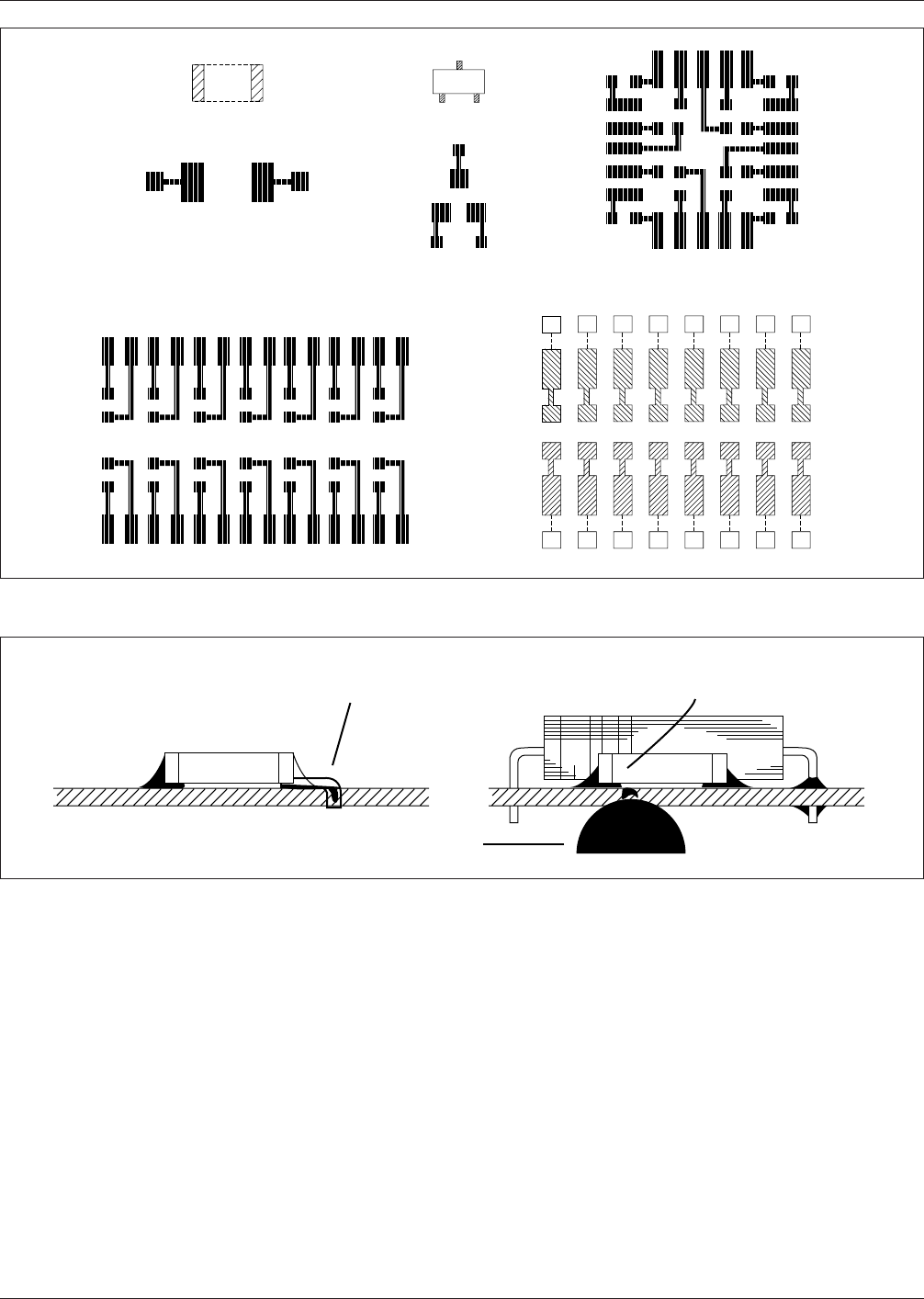
IPC-782-3-25
Figure 3–25 Examples of via positioning concepts
Side 2
Vias
Side 1
Vias
Side 1
Vias
Side 2
Vias
Chip component
Chip component
PLCC
SOIC
SOIC
IPC-782-3-26
Figure 3–26 Vias under components
Caution
Solder
Characteristic
Solder
Migration
▼
▼
Wave Solder
▼
IPC-SM-782A December 1999
30
电子技术应用 www.ChinaAET.com
IPC-782-3-27
Figure 3–27 Conductor characteristics
▼
LaminateX
▼
Etch Factor =
V
X
An etch factor of 1/1 is usually considered practical.
Higher factors may be specified for some applications.
Resist
▼
V
▼
▼
"B" (DCW)
"E" Outgrowth
▼
▼
▼
▼
▼
▼
▼
"C" Undercut
▼
"A"
(MCW)*
Overhang
Panel Plating (Liquid Resist)
▼
▼
(OCW)*
▼
▼
"D"
"B" (DCW)*
"E" Outgrowth
▼
▼
(MCW)*
"A"
▼
▼
Pattern Plating (Liquid Resist)
▼
"B" (DCW)
(MCW)*
"C" Undercut
& Overhang
Panel Plating (Dry Film Resist)
▼
▼
"A"
▼
▼
▼
▼
▼
"D"
▼
"A"
(MCW)*
Overhang
Pattern Plating (Dry Film Resist)
▼
▼
▼
(OCW)*
"B" (DCW)*
▼
▼
▼
▼
"E" Outgrowth
▼
▼
"C" Undercut
▼
▼
"B" (DCW)*
▼
"C" Undercut
▼
Thin Clad & Pattern Plating (Dry Film Resist)
A = MCW (Minimum Conductor Width) B = DCW (Desi
g
n Conductor Width) D = OCW (Overall Conductor Width
Table 3–8 Typical Values to Be Added or Subtracted to Nominal Production to Achieve Desired Nominal Conductor Width
Description
1/2 Oz. Copper 1 Oz. Copper 2 Oz.Copper
Panel Pattern Panel Pattern Panel Pattern
Screen
Liquid
Photo
Dry
Film
Photo Screen
Liquid
Photo
Dry
Film
Photo Screen
Liquid
Photo
Dry
Film
Photo Screen
Liquid
Photo
Dry
Film
Photo Screen
Liquid
Photo
Dry
Film
Photo Screen
Liquid
Photo
Dry
Film
Photo
Subtractive
Method
Simple Etch
+25µm
[+0.0010]
+25µm
[+0.0010]
+25µm
[+0.0010]
— — — +38µ
[+0.0015]
+38µm
[+0.0015]
+38µm
[+0.0015]
— — — +63µm
[+0.0025]
+63µm
[+0.0025]
+63µm
[+0.0025]
———
Bare Copper
[PTH]
+38µ
[+0.0015]
+38µm
[+0.0015]
+50µm
[+0.0020]
-25µ
[-0.0010]
-25µm
[-0.0010]
-25µm
[-0.0010]
+50µm
[+0.0020]
+50µm
[+0.0020]
+63µm
[+00025]
0 0 +50µm
[+0.0020]
+76µm
[+0.0030]
+76µm
[+0.0030]
+89µm
[+0.0035]
+38µm
[+0.0015]
+38µm
[+0.0015]
+89µm
[+0.0035]
Tin-Lead
[PTH]
+38µm
[+0.0015]
+38µm
[+0.0015]
+50µm
[+0.0020]
-25µm
[-0.0010]
-25µm
[-0.0010]
+25µm
[+0.0010]
+50µm
[+0.0020]
+50µm
[+0.0020]
+63µm
[+0.0025]
0 0 +50µm
[+0.0020]
+76µm
[+0.0030]
+76µm
[+0.0030]
+89µm
[+0.0035]
+38µm
[+0.0015]
+38µm
[+0.0015]
+89µm
[+0.0035]
Gold Nickel
[PTH]
+38µm
[+0.0015]
+38µm
[+0.0015]
+50µm
]+0.0020]
-25µm
[-0.0010]
-25µm
[-0.0010]
+25µm
[+0.0010]
+50µm
[+0.0020]
+50µm
[+0.0020]
+63µm
[+0.0025]
0 0 +50µm
[+0.0020]
+76µm
[+0.0030]
+76µm
[+0.0030]
+89µm
[+0.0035]
+38µm
[+0.0015]
+38µm
[+0.0015]
+89µm
[+0.0015]
For Deposited Copper Thickness Equivalents
Additive
Method
Electroless
Copper
No-Etch
— — — -50µ
[-0.0020]
-25µm
[-0.0010]
-0µm
[0.0000]
— — — -76µm
[-0.0030]
-50µ
[-0.0020]
-0µ
[-0.0000]
— — — -101µ
[-0.0040]
-76µm
[-0.0030]
-0µm
[-0.0000]
Semi Additive
Method
Copper-No
Overplate
— — — -50µm
[-0.0020]
-25µm
[-0.0010]
-0µm
[-0.0000]
— — — -76µm
[-0.0030]
-50µm
[-0.0020]
-0µm
[-0.0000]
— — — -101µm
[-0.0040]
-76µm
[-0.0030]
-0µm
[-0.0000]
Tin Lead
Overplate
— — — -76µm
[-0.0030]
-50µm
[-0.0020]
-25µm
[-0.0010]
— — — -101µ
[-0.0040]
-76µm
[-0.0030]
-25µm
[-0.0010]
— — — -127µm
[-0.0050]
-101µm
[-0.0040]
-25µm
[-0.0010]
December 1999 IPC-SM-782A
31
电子技术应用 www.ChinaAET.com
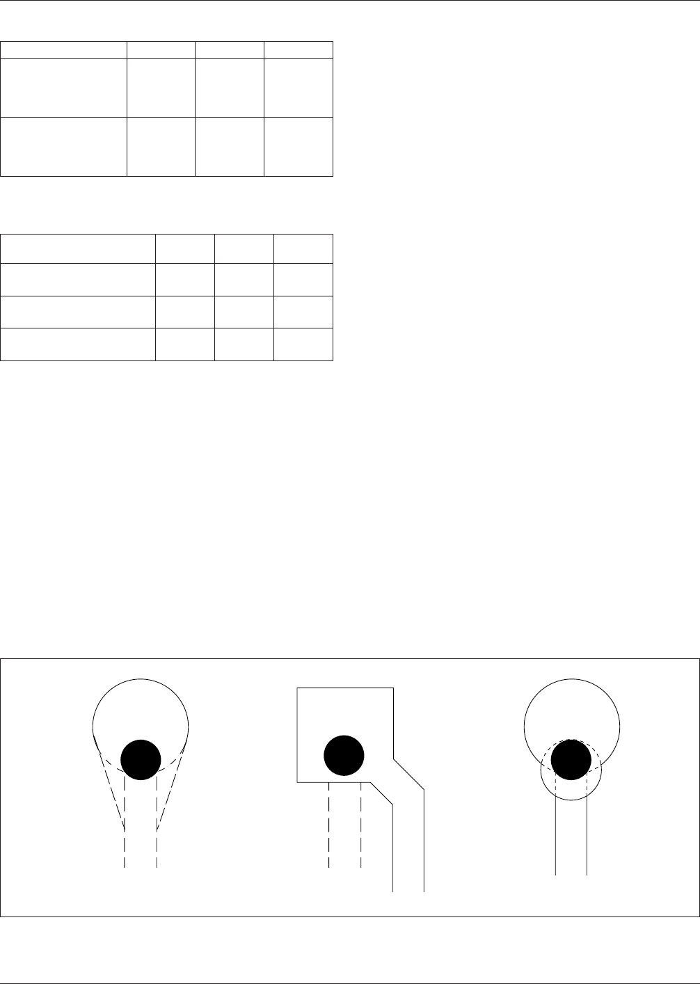
result is a scrapped PB. Since signal conductors intersect
the lands from all directions, any breakout has the poten-
tial to randomly disconnect conductors all over the PB.
Maintaining consistent annular ring control is difficult at
best, another method had to be developed to insure connec-
tivity between lands and conductors. This method is called
filleting, corner entry or keyholing. Explained simply, each
method is intended to provide excess original copper mate-
rial at the junction where the conductor enters the land. The
land which is filleted resembles a teardrop; it is square for
the corner entry, and looks like a figure eight for keyhol-
ing. All features point in the direction of the conductor to
permit additional misregistration allowances (see Figure
3–28).
3.6.4.5 Fabrication Panel Format
Components can be
mounted on individual boards or on boards that are still
organized in panel form. Boards or panels that will be
moved by automatic handling equipment or pass through
automated operations, (parts placement, soldering, clean-
ing, etc.) must have the sides kept free of parts or active
circuitry. Special tooling and fixturing holes are generally
located within the edge clearance areas. The clearance
areas are needed to avoid interference with board handling
fixtures, guidance rails and alignment tools.
Typically a clear area of 3.0 to 5.0 mm [0.118 to 0.200 in]
must be allowed along the sides for the clearance. The
required clearance width is dependent upon the design of
the board handling and fixturing equipment. These dimen-
sions should be obtained from the equipment manufacturer
before board or panel design. (See Figure 3–29.)
For accurate fixturing, a minimum of two (and preferably
four) nonplated holes are located in the corners of the
board to provide accurate mechanical registration on board
transfer equipment. Board handling holes (typically 3.2
mm [0.125] diameter) may also be located in the clearance
areas. These holes are used by automated board handling
equipment to move boards (or panels) from station to sta-
tion in automated assembly lines. Specific sizes should be
obtained from the equipment manufacturer. In addition,
optical fiducial marks may be located near the fixturing
holes if optical alignment is used, to improve registration
(see Figure 3–14).
3.6.4.6 Board Size and Panel Construction
In order to
fully utilize the automation technology associated with sur-
face mount components, a designer should consider how a
printed board or P&I structure will be fabricated,
assembled and tested. Each of these processes, because of
the particular equipment used, requires fixturing which will
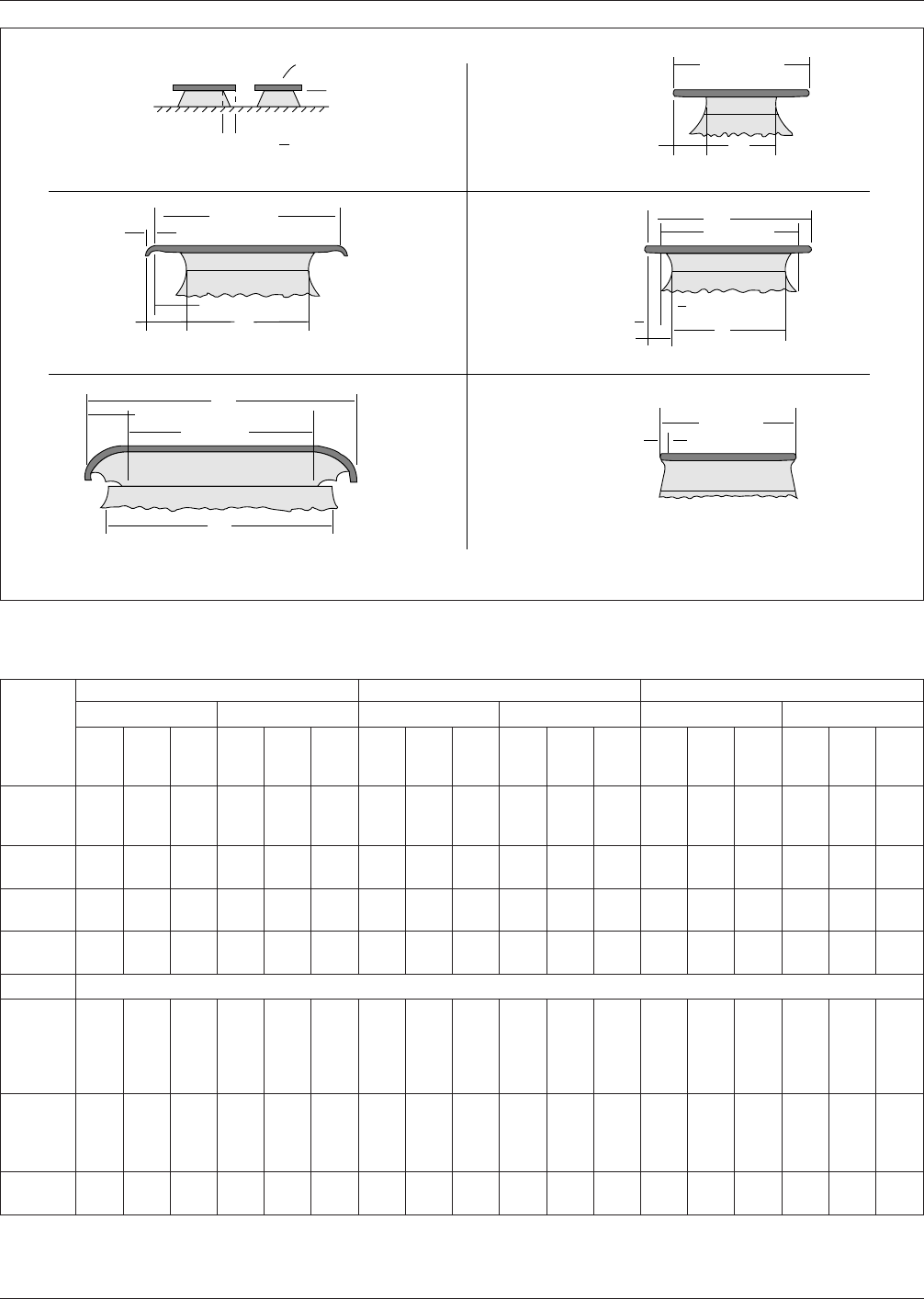
Table 3–9 Conductor Width Tolerances
Feature Level A Level B Level C
Without plating +0.05
–0.10
[+0.002]
[–0.004]
+0.03
–0.05
[+0.001]
[–0.002]
+0.02
–0.04
[+0.0008]
[–0.0016]
With plating +0.10
–0.10
[+0.004]
[–0.004]
+0.08
–0.08
[+0.003]
[–0.003]
+0.05
–0.05
[+0.002]
[–0.002]
Table 3–10 Conductive Pattern Location Tolerances
Greatest Board/
X, Y Dimension Level A Level B Level C
Up to 300 mm [12.0] 0.30 mm
[0.012]
0.20 mm
[0.008]
0.10 mm
[0.004]
Up to 450 mm [18.0] 0.40 mm
[0.016]
0.30 mm
[0.012]
0.20 mm
[0.008]
Up to 600 mm [24.0] 0.40 mm
[0.016]
0.30 mm
[0.012]
0.20 mm
[0.008]
IPC-782-3-28
Figure 3–28 Examples of modified landscapes
Corner EntryFilleting
Key
Holing
IPC-SM-782A December 1999
32
电子技术应用 www.ChinaAET.com