IPC-SM-782A 表面安装设计和焊盘设计标准(带BGA).pdf - 第42页
exposed or damaged, and rough edges must be sanded lightly to remove burrs and rough fabric particles. See Fig- ure 3–30. The routed slot and tab pattern is widely used for panel construction and break-away tab extension…
affect or dictate certain facets of the board layout. Tooling
holes, panel size, component orientation and clearance
areas (both component and conductor) on the primary and
secondary sides of the board are all equipment and process
dependent.
To produce a cost effective layout through optimum base
material utilization a designer should consult with the
board fabricator to determine optimum panel size. The
board should be designed to utilize the manufacturer’s sug-
gested usable area. Smaller boards can be ganged or nested
on this same panel size to simplify fixturing and reduce
excessive handling during assembly. Most manufacturers
will suggest various methods of retaining assemblies in
panels. A method should be chosen taking the assembly
and test processes into consideration.
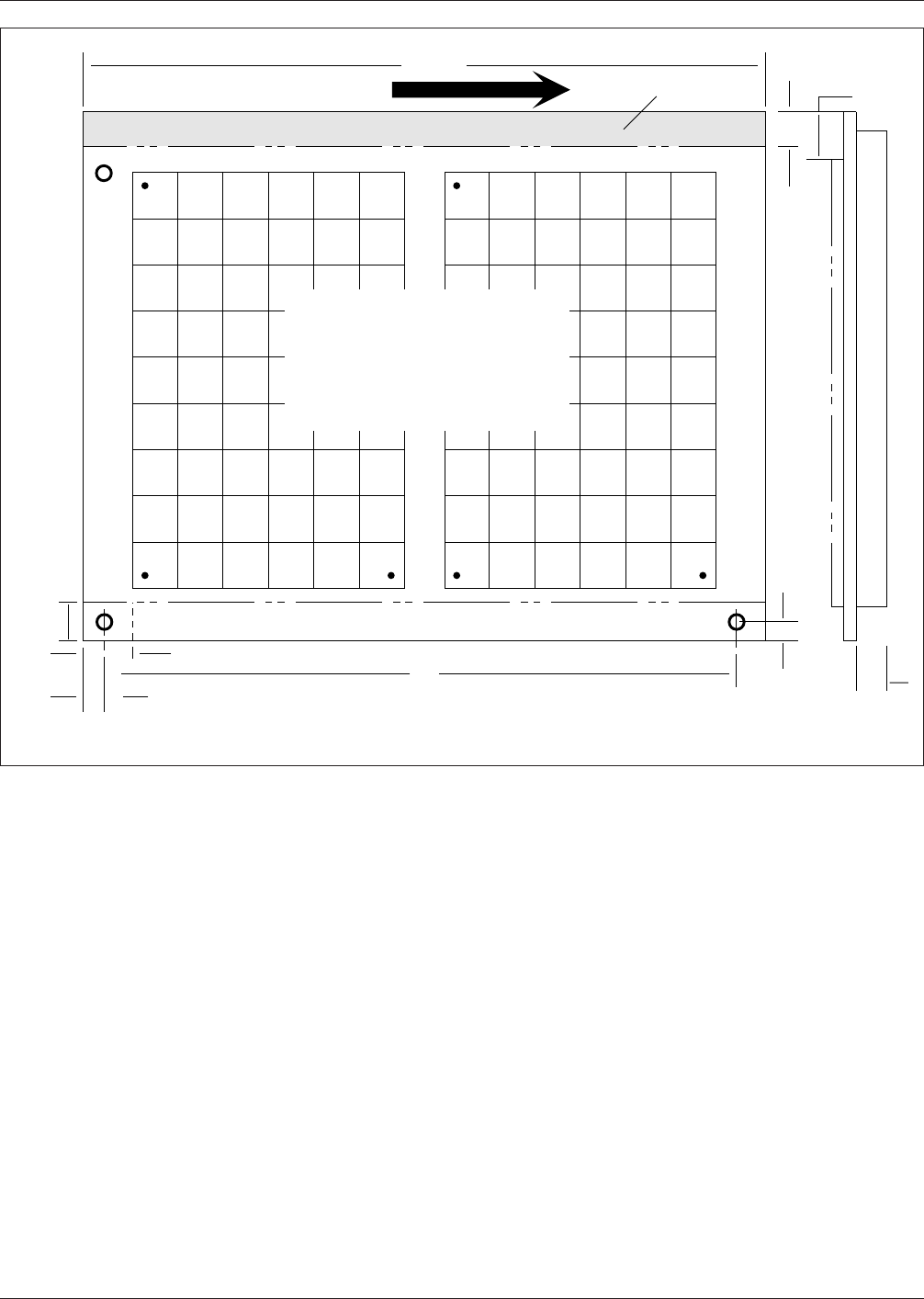
Figure 3–29 shows the typical use of a copper clad glass
laminate panel. See IPC-D-322 for panel to board relation-
ship.
Small boards can effectively be arranged on a single work-
ing panel, if the designer works closely with manufactur-
ing. These are commonly called nested panels or pallets.
Panel construction may include several boards arranged in
a matrix or simply one board requiring additional material
retained for efficient assembly processing. The large board
or several smaller boards are retained in the panels and
separated after all assembly processes are completed.
Excising or separating the individual boards from the panel
must be planned as well. Several methods are used to retain
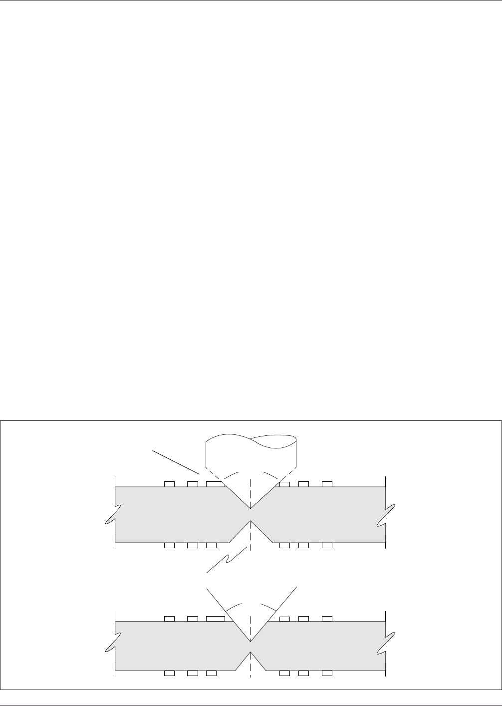
circuits in a panel, including V-groove scoring and routed
slot with break-away tabs.
V-groove scoring is generally provided on both surfaces of
the board, and only in a straight line. A small cross section
of board material is retained at the break line. An allow-
ance for the scoring angle must be made as well. Conduc-
tors that are located too close to the score groove will be
IPC-782-3-29
Figure 3–29 Typical copper glass laminate panel
▼
The keepout zone defined in this illustration is typical for in-line assembly automation using reflow and wave solder processes.
▼
X
Typical Finished Panel
for Automated SMT
Assembly Equipment
Showing two
printed board assemblies
▼
300mm
[12.0]
▼
▼
3.0mm
[0.12]
▼
▼
5.0mm
[.2.0]
▼
10mm [0.40]
▼
5mm [0.20]
▼▼
▼
3.0mm
[0.12]
Keep Clear
▼
Primary Component Side
Secondary Component Side
▼
▼
12.0mm
max.
[0.500]
5mm
[2.0] min.
DIRECTION OF FLOW
KEEPOUT ZONE
KEEPOUT ZONE
▼
▼
▼
December 1999 IPC-SM-782A
33
电子技术应用 www.ChinaAET.com
exposed or damaged, and rough edges must be sanded
lightly to remove burrs and rough fabric particles. See Fig-
ure 3–30.
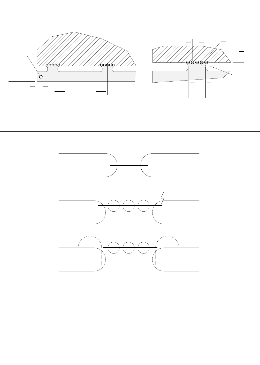
The routed slot and tab pattern is widely used for panel
construction and break-away tab extensions. Routing is
more precise than scoring, and edge surfaces are smooth,
but the break-away ‘‘tab’’ points will require consideration.
Tabs can be cut and ground flush with the board edge or
pre-drilled in a pattern. The drilled pattern furnishes a low
stress break point on the ‘‘tab’’. If the hole pattern is
recessed within the board edge, secondary sanding or
grinding can be bypassed. See Figures 3–31 and 3–32.
3.6.4.7 Artwork Compensation and Scaling
Artwork
compensation and scaling are two adjustments that are
made by the printed board fabricator to the original printed
board artwork film or CAD data prior to beginning the fab-
rication process.
Modifications are made to the artwork feature sizes to com-
pensate for the etch factor that occurs when etching away
unwanted copper from the inner and outer layers of a
printed board. The outer layers require more compensation
than inner layers due to the overplating of copper and other
metals that form the copper protection during the etching
process. This is one of the reasons conductor width control
on outer layers of printed boards can be substantially more
difficult than inner layer conductor width control.
Scaling is an adjustment made to the artwork by the fabri-
cator offset printed board material shrinkage, which is in
the range of 8–13 µm [0.00035–0.0005 in] per 25 mm, that
occurs during the lamination process. When the annular
ring requirements fall below a nominal 0.25 mm [0.010 in],
artwork scaling will typically be invoked by the printed
board fabricator.
3.7 Outer Layer Finishes
3.7.1 Soldermask vs. Lands Only
In referring to the
outer layers of the multilayer PB, there is a dramatic dif-
ference between the concepts of soldermask and having no
conductors on the outer layers. Conventional SMT design
rules allow routing conductors on the outer layers, running
the conductors between Surface Mount lands, then apply-
ing soldermask to cover the conductors and leave the lands
exposed. For high density SMT applications, the conduc-
tors and clearances on the outer layers are generally in the
0.15–0.2 mm [0.006–0.008 in] range.
Aside from the soldermask registration, maintaining preci-
sion conductor width control on the outer layers is signifi-
cantly more difficult than on the inner layers. Outer layer
conductor integrity can be a cause of poor fabrication
yields. The soldermask rule is very simple: the conductors
between lands must be covered with soldermask, while the
lands must not have any soldermask on them. When using
smaller geometries, adding the Standard Fabrication Allow-
ance of 0.2 mm [0.008 in] can make soldermask registra-
tion very difficult.
Given the two distinct yield difficulties of conductor width
control and soldermask application, board manufacturers
with experience in high density SMT printed conductor
IPC-782-3-30
Figure 3–30 Conductor clearance for V-groove scoring
90°
▼
▼
Break Line
▼
60°
▼
▼
Conductors Must
Be Clear of Score
Zone
90° Score
Option
60° Score
Option
▲
IPC-SM-782A December 1999
34
电子技术应用 www.ChinaAET.com
boards may favor the lands only (pad cap) concept. The
pad cap concept has two yield improvement benefits: 1) no
fine conductor geometries on the outer layers because they
are buried in the inner layers where conductor width con-
trol is significantly easier, and 2) the need for soldermask
is reduced or eliminated because there are no small spaces
to protect from the soldering process.
In general, an 8-layer printed board, with lands only on the
outer layer, is similar in cost to a 6-layer printed board with
solder mask, assuming both have SMT geometries. The
primary reason for this is that some PB fabricators are
realizing about a 12% yield improvement by not having the
fine line conductors on the outer layers.
The benefits of pad caps continue into the assembly pro-
cess by increasing yields through the reduction of solder
shorts or bridging. The pad cap concept provides 100%
testability, thus testing benefits are both economical and
practical.
IPC-782-3-31
Figure 3–31 Breakaway (routed pattern)
[75mm 3.0] TYP
Approximately
Center to Center Spacing
▼
▼
▼
▼ ▼
▼
▼
▼
▼
0.4mm
[0.159]
Tooling Hole
5.0mm
[0.197]
10mm [0.40]
Depending on PWB
Outline Design
5.0mm
[0.197]
12.5mm
[0.50]
Breakaways
▼
▼
▼
▼
▼
1.25mm [0.050] TYP
0.8mm [0.031]
Dia Thru XX PL
▼
▼
▼
▼
2.25mm
[0.90]
1.2mm [0.047]
R TYP
4.5mm
[0.180]
REF
Detail of Breakaway
▼
▼
0.4mm
[.016]
LOW STRESS (MOUSE BITE) BREAKAWAY
IPC-782-3-32
Figure 3–32 Routed slots
Break Line
▼
December 1999 IPC-SM-782A
35
电子技术应用 www.ChinaAET.com