IPC-SM-782A 表面安装设计和焊盘设计标准(带BGA).pdf - 第90页
6.0 TOLERANCE AND SOLDER JOINT ANALYSIS Figure 4 provides an analysis of tolerance assumptions and resultant solder joints based on the land pattern dimensions shown in Figure 3. Tolerances for the component dimensions, …
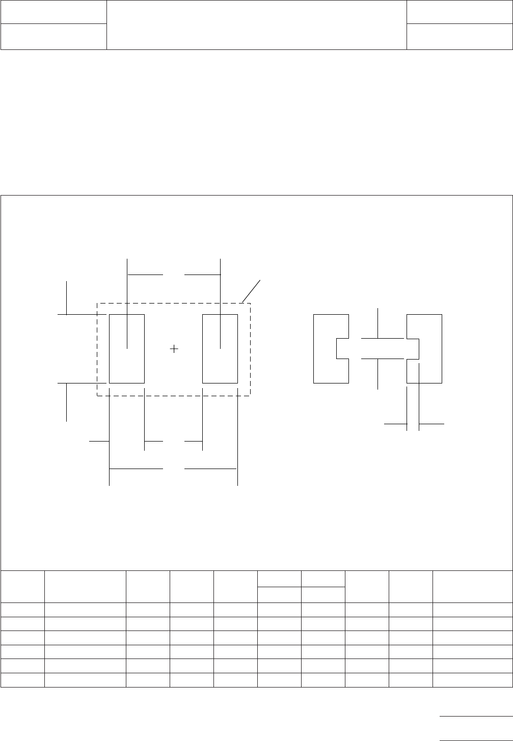
5.0 LAND PATTERN DIMENSIONS
Figure 3 provides the land pattern dimensions for metal elec-
trode face components (MELFs). These numbers represent
industry consensus on the best dimensions based on empiri-
cal knowledge of fabricated land patterns.
In the table, the dimensions shown are at maximum material
condition (MMC). The least material condition (LMC) should
not exceed the fabrication (F) allowance shown on page 4.
The LMC and the MMC provide the limits for each dimension.
The dotted line in Figure 3 shows the grid placement court-
yard which is the area required to place land patterns and
their respective components in adjacent proximity without
interference or shorting. Numbers in the table represent the
number of grid elements (each element is 0.5 by 0.5 mm) in
accordance with the international grid detailed in IEC publica-
tion 97.
RLP No.
Component
Identifier (mm) [in] Z (mm) G (mm) X (mm)
Y (mm) C (mm)
AB
Placement Grid
(No. of Grid
Elements)ref ref
200A SOD-80/MLL-34 4.80 2.00 1.80 1.40 3.40 0.50 0.50 6x12
201A SOD-87/MLL-41 6.30 3.40 2.60 1.45 4.85 0.50 0.50 6x14
202A 2012 [0805] 3.20 0.60 1.60 1.30 1.90 0.50 0.35 4x8
203A 3216 [1206] 4.40 1.20 2.00 1.60 2.80 0.50 0.55 6x10
204A 3516 [1406] 4.80 2.00 1.80 1.40 3.40 0.50 0.55 6x12
205A 5923 [2309] 7.20 4.20 2.60 1.50 5.70 0.50 0.65 6x18
Figure 3 Metal electrode face component land pattern dimensions
▼
▼
▼
▼
▼
▼
▼
▼
▼
C
G
Z
X
Y
▼
▼
▼
▼
A
Optional detent pattern
B
▼
Grid placement
courtyard
IPC-782-8-5-3
IPC-SM-782
Subject
Metal Electrode Face (MELF) Components
Date
5/96
Section
8.5
Revision
A
Page3of4
电子技术应用 www.ChinaAET.com
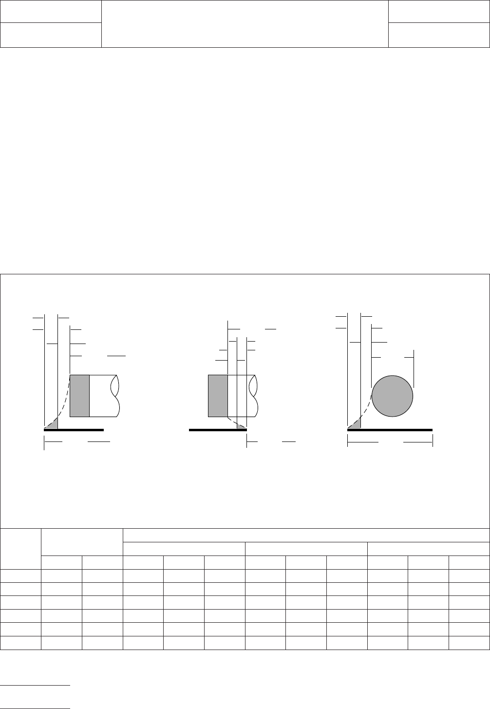
6.0 TOLERANCE AND SOLDER JOINT ANALYSIS
Figure 4 provides an analysis of tolerance assumptions and
resultant solder joints based on the land pattern dimensions
shown in Figure 3. Tolerances for the component dimensions,
the land pattern dimensions (fabrication tolerances on the
interconnecting substrate), and the component placement
equipment accuracy are all taken into consideration.
Figure 4 provides the solder joint minimums for toe, heel, and
side fillets, as discussed in Section 3.3. The tolerances are
addressed in a statistical mode, and assume even distribution
of the tolerances for component, fabrication, and placement
accuracy.
Individual tolerances for fabrication (‘‘F’’) and component
placement equipment accuracy (‘‘P’’) are assumed to be as
given in the table. These numbers may be modified based on
user equipment capability or fabrication criteria. Component
tolerance ranges (C
L
,C
S
, and C
W
) are derived by subtracting
minimum from maximum dimensions given in Figure 2. The
user may also modify these numbers, based on experience
with their suppliers. Modification of tolerances may result in
alternate land patterns (patterns with dimensions other than
the IPC registered land pattern dimensions).
The dimensions for minimum solder fillets at the toe, heel, or
side (J
T
,J
H
,J
S
) have been determined based on industry
empirical knowledge and reliability testing. Solder joint
strength is greatly determined by solder volume. An observ-
able solder fillet is necessary for evidence of proper wetting.
Thus, the values in the table usually provide for a positive sol-
der fillet. Nevertheless, the user may increase or decrease the
minimum value based on process capability.
RLP No.
Tolerance
Assumptions (mm)
Solder Joint
Toe (mm) Heel (mm) Side (mm)
FPC
L
J
T
min J
T
max C
S
J
H
min J
H
max C
W
J
S
min J
S
max
200A 0.10 0.10 0.40 0.54 0.96 0.45 0.09 0.56 0.10 0.01 0.19
201A 0.10 0.10 0.40 0.54 0.96 0.45 0.19 0.66 0.10 -0.01 0.17
202A 0.10 0.10 0.20 0.53 0.77 0.28 0.26 0.58 0.10 0.04 0.21
203A 0.10 0.10 0.40 0.49 0.91 0.45 0.32 0.79 0.10 0.04 0.21
204A 0.10 0.10 0.40 0.54 0.96 0.45 0.07 0.54 0.10 0.04 0.21
205A 0.10 0.10 0.40 0.54 0.96 0.45 0.07 0.54 0.10 0.01 0.19
Figure 4 Tolerance and solder joint analysis
Wmin
Lmin
▼
▼
Zmax
▼
▼
1
/2 T
T
J
T
min
Zmax = Lmin + 2J
T
min + T
T
Where:
J
T
min = Minimum toe fillet
T
T
= Combined tolerances
at toe fillet
Smax
J
H
min
Gmin = Smax - 2J
H
min - T
H
Where:
J
H
min = Minimum heel fillet
T
H
= Combined tolerances
at heel fillet
1
/2 T
H
Xmax
Xmax = Wmin + 2J
S
min
+ T
S
Where:
J
S
min = Minimum side fillet
T
S
= Combined tolerances
at side fillet
▼
▼
Toe Fillet
1
/2 T
S
▼
▼
▼
Heel Fillet Side Fillet
▼
▼
▼
▼
▼
J
T
max
J
H
max
J
S
max
J
S
min
▼
▼
▼
▼
▼
▼
▼
▼
▼
▼
▼
▼
▼
▼
▼
▼
▼
▼
Gmin
▼
▼
IPC-782-8-5-4
IPC-SM-782
Subject
Metal Electrode Face (MELF) Components
Date
5/96
Section
8.5
Revision
A
Page4of4
电子技术应用 www.ChinaAET.com
1.0 SCOPE
This subsection provides the component and land pattern
dimensions for SOT 23 (small outline transistor) components.
Basic construction of the SOT 23 device is also covered. At
the end of this subsection is a listing of the tolerances and
target solder joint dimensions used to arrive at the land pat-
tern dimensions.
2.0 APPLICABLE DOCUMENTS
See Section 8.0 for documents applicable to the subsections.
3.0 COMPONENT DESCRIPTIONS
One of the first active devices in packaged form for surface
mounting was the SOT device. Plastic encapsulated three ter-
minal devices with leads formed out from the body were sur-
face mounted to overcome some of the problems and difficul-
ties in handling dip transistors. In general, SOT packages are
used with diodes, transistors, and small I/O devices.
The SOT 23 package is the most common three-lead surface
mount configuration.
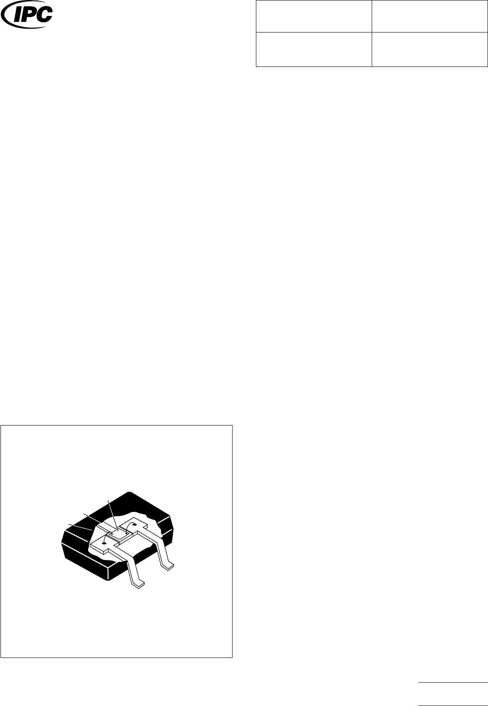
3.1 Basic Construction
The SOT 23 package has had
several redesigns to meet the needs of both hybrid and
printed board surface mount industries. These changes
resulted in low, medium and high profile characteristics which
basically reflect the clearance that the body is from the mount-
ing surface. See Figure 1 for construction characteristics and
Figure 2 for dimensions.
3.1.1 Termination Materials
Leads should be solder-
coated with a tin/lead alloy. The solder should contain
between 58 to 68% tin. Solder may be applied to the leads by
hot dipping or by plating from solution. Plated solder termina-
tions should be subjected to post-plating reflow operation to
fuse the solder. The tin/lead finish should be at least 0.0075
mm [0.0003 in] thick.
Solder finish applied over precious metal electrodes should
have a diffusion barrier layer between the electrode metalliza-
tion and the solder finish. The barrier layer should be nickel or
an equivalent diffusion barrier, and should be at least 0.00125
mm [0.00005 in] thick.
3.1.2 Marking
Parts are available with or without marked
values.
3.1.3 Carrier Package Format
Carrier package format
shall be according to the following: body type TO-236, 8 mm
tape/4 mm pitch.
3.1.4 Resistance to Soldering
Parts should be capable of
withstanding five cycles through a standard reflow system
operating at 215°C. Each cycle shall consist of 60 seconds
exposure at 215°C. Parts must also be capable of withstand-
ing a minimum of 10 seconds immersion in molten solder at
260°C.
IPC-782-8-6-1
Figure 1 SOT 23 construction
Passivated
Semiconductor Chip
Collector lead
Bonding wire
Epoxy body
Emitter lead
Base lead
IPC-SM-782
Surface Mount Design
and Land Pattern Standard
Date
8/93
Section
8.6
Revision Subject
SOT 23
Page1of4
电子技术应用 www.ChinaAET.com