IPC-SM-782A 表面安装设计和焊盘设计标准(带BGA).pdf - 第75页
1.0 SCOPE Microminiature leadless devices are available to the circuit designer in rectangular form for discrete components such as chip capacitors. This subsection provides the component and land pattern dimensions for …
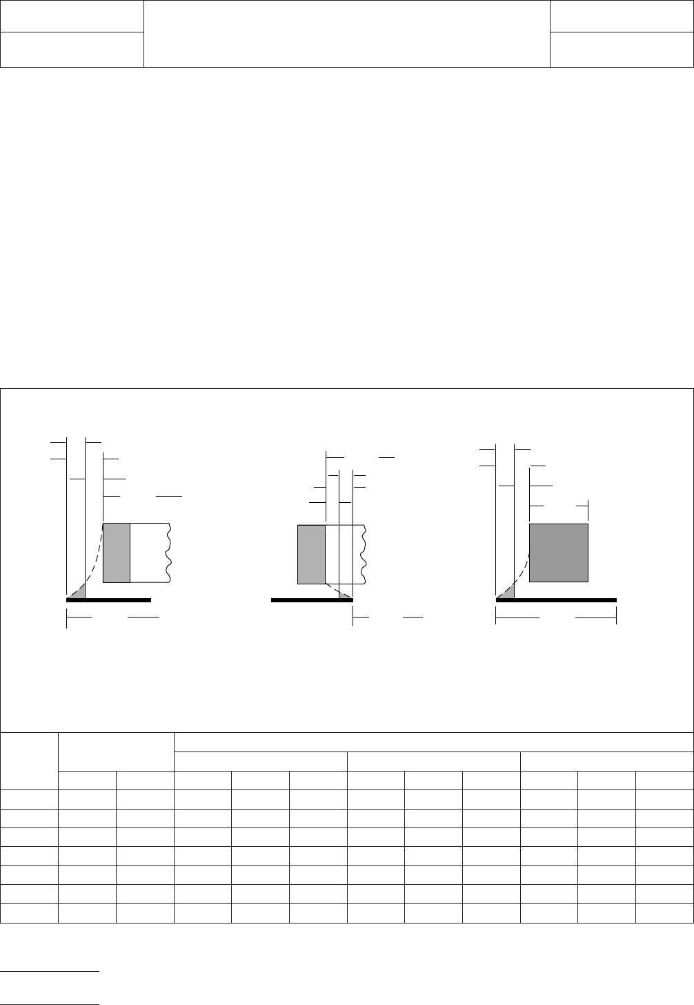
6.0 TOLERANCE AND SOLDER JOINT ANALYSIS
Figure 4 provides an analysis of tolerance assumptions and
resultant solder joints based on the land pattern dimensions
shown in Figure 3. Tolerances for the component dimensions,
the land pattern dimensions (fabrication tolerances on the
interconnecting substrate), and the component placement
equipment accuracy are all taken into consideration.
Figure 4 provides the solder joint minimums for toe, heel, and
side fillets, as discussed in Section 3.3. The tolerances are
addressed in a statistical mode, and assume even distribution
of the tolerances for component, fabrication, and placement
accuracy.
Individual tolerances for fabrication (‘‘F’’) and component
placement equipment accuracy (‘‘P’’) are assumed, and are
given in the table. These numbers may be modified based on
user equipment capability or fabrication criteria. Component
tolerance ranges (C
L
,C
S
and C
W
) are derived by subtracting
minimum from maximum dimensions given in Figure 2. The
user may also modify these numbers, based on experience
with their suppliers. Modification of tolerances may result in
alternate land patterns (patterns with dimensions other than
the IPC registered land pattern dimensions.)
The dimensions for the statistical minimum and maximum sol-
der joint fillets at the toe, heel, or side (J
T
,J
H
,orJ
S
) have been
determined based on the equations detailed in Section 3.3.
Solder joint strength is greatly determined by solder volume.
An observable solder fillet is necessary for evidence of proper
wetting. Thus, the values in the table usually provide for a
positive solder fillet. Nevertheless, the user may increase or
decrease the minimum value based on process capability.
RLP No.
Tolerance (mm)
Assumptions
Solder Joint
Toe (mm) Heel (mm) Side (mm)
FPC
L
J
Tmin
J
Tmax
C
S
J
Hmin
J
Hmax
C
W
J
Smin
J
Smax
100A 0.10 0.10 0.10 0.51 0.60 0.30 –0.02 0.15 0.12 0.02 0.11
101A 0.10 0.10 0.20 0.53 0.65 0.41 0.04 0.25 0.25 0.01 0.15
102A 0.10 0.10 0.30 0.51 0.68 0.77 –0.03 0.36 0.30 0.03 0.20
103A 0.10 0.10 0.30 0.51 0.68 0.77 0.17 0.56 0.30 0.01 0.18
104A 0.10 0.10 0.30 0.51 0.68 0.77 0.17 0.56 0.30 0.01 0.18
105A 0.10 0.10 0.30 0.51 0.68 0.77 0.27 0.66 0.30 0.01 0.18
106A 0.10 0.10 0.30 0.46 0.63 0.77 0.32 0.71 0.30 –0.09 0.08
Figure 4 Tolerance and solder joint analysis
Wmin
Lmin
▼
▼
Zmax
▼
▼
1
/2 T
T
J
T
min
Zmax = Lmin + 2J
T
min + T
T
Where:
J
T
min = Minimum toe fillet
T
T
= Combined tolerances
at toe fillet
Smax
J
H
min
Gmin = Smax - 2J
H
min - T
H
Where:
J
H
min = Minimum heel fillet
T
H
= Combined tolerances
at heel fillet
1
/2 T
H
Xmax
Xmax = Wmin + 2J
S
min + T
S
Where:
J
S
min = Minimum side fillet
T
S
= Combined tolerances
at side fillet
▼
▼
Toe Fillet
1
/2 T
S
▼
▼
▼
Heel Fillet Side Fillet
▼
▼
▼
▼
▼
J
T
max
J
H
max
J
S
max
J
S
min
▼
▼
▼
▼
▼
▼
▼
▼
▼
▼
▼
▼
▼
▼
▼
▼
▼
▼
Gmin
▼
▼
IPC-782-8-1-4
IPC-SM-782
Subject
Chip Resistors
Date
5/96
Section
8.1
Revision
A
Page4of4
电子技术应用 www.ChinaAET.com
1.0 SCOPE
Microminiature leadless devices are available to the circuit
designer in rectangular form for discrete components such as
chip capacitors.
This subsection provides the component and land pattern
dimensions for chip capacitors, along with an analysis of tol-
erance and solder joint assumptions used to arrive at the land
pattern dimensions. Basic construction of the chip capacitor
is also covered.
2.0 APPLICABLE DOCUMENTS
See Section 8.0 for documents applicable to the subsections.
3.0 COMPONENT DESCRIPTIONS
A variety of values exist for capacitors. The following sections
describe the most common types.
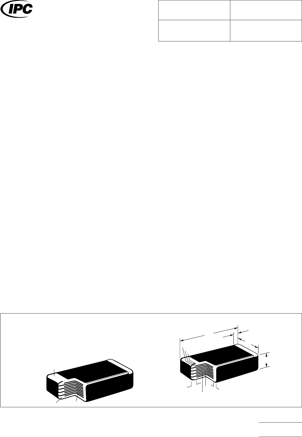
3.1 Basic Construction
Multilayer ceramic capacitors use
substrate materials such as alumina for hybrid circuits and
porcelainized metal. The monolithic construction used in pro-
ducing these chips results in a solid block of ceramic with an
enclosed electrode system and metallized ends for circuit
attachment. This solid block is rugged and capable of with-
standing the harsh environment and treatment associated
with manufacturing processes. See Figure 1.
Electrodes are given a common terminal by coating the chip
ends with a precious metal-glass formulation suspended in an
organic vehicle. Consecutive drying and firing eliminates the
organic components and effects a bond between the ceramic
dielectric and glass constituent in the termination.
3.1.1 Termination Materials
End terminations should be
solder coated with a tin/lead alloy. The solder should contain
between 58 to 68% tin. Solder may be applied to the termi-
nation by hot dipping or by plating from solution. Plated sol-
der terminations should be subjected to a post-plating reflow
operation to fuse the solder. The tin/lead finish should be at
least 0.0075 mm [0.0003 in] thick.
The termination shall be symmetrical, and shall not have nod-
ules lumps, protrusions, etc., that compromise the symmetry
or dimensional tolerances of the part. The end termination
shall cover the ends of the components, and shall extend out
to the top and bottom of the component.
Most common termination materials include palladium-silver
alloy, silver, and gold. Solder finish applied over precious
metal electrodes shall have a diffusion-barrier layer between
the electrode metallization and the solder finish. The barrier
layer should be nickel or an equivalent diffusion barrier, and
should be at least 0.00125 mm [0.00005 in] thick.
3.1.2 Marking
Ceramic capacitors are typically unmarked.
3.1.3 Carrier Package Format
Bulk rods, 8 mm tape/4
mm pitch is preferred for best handling. Tape and reel speci-
fications provide additional requirements.
3.1.4 Resistance to Soldering
Parts should be capable of
withstanding five cycles through a standard reflow system
operating at 215°C. Each cycle shall consist of 60 seconds
exposure at 215°C. Parts must also be capable of withstanding a
minimum of 10 seconds immersion in molten solder at 260°C.
Caution should be exercised when using the 4564 (1825)
capacitor mounted on organic substrates due to CTE mis-
match if the assembly sees wide temperature swings in the
assembly process or end use.
IPC-782-8-2-1
Figure 1 Chip capacitor construction
1. Termination
2. Dielectric
3. Electrode
4. Chip length
5."A" electrode print
6. Electrode print
7. Cap (Topping layer)
8. End margin
9. Base layer
10. Shim (Active dielectric layer)
11. Side margin
12. Chip thickness
13. Chip width
14. Termination width
1
2 3
5
6
7
8
9
10
11
4
14
13
12
IPC-SM-782
Surface Mount Design
and Land Pattern Standard
Date
5/96
Section
8.2
Revision
A
Subject
Chip Capacitors
Page1of4
电子技术应用 www.ChinaAET.com
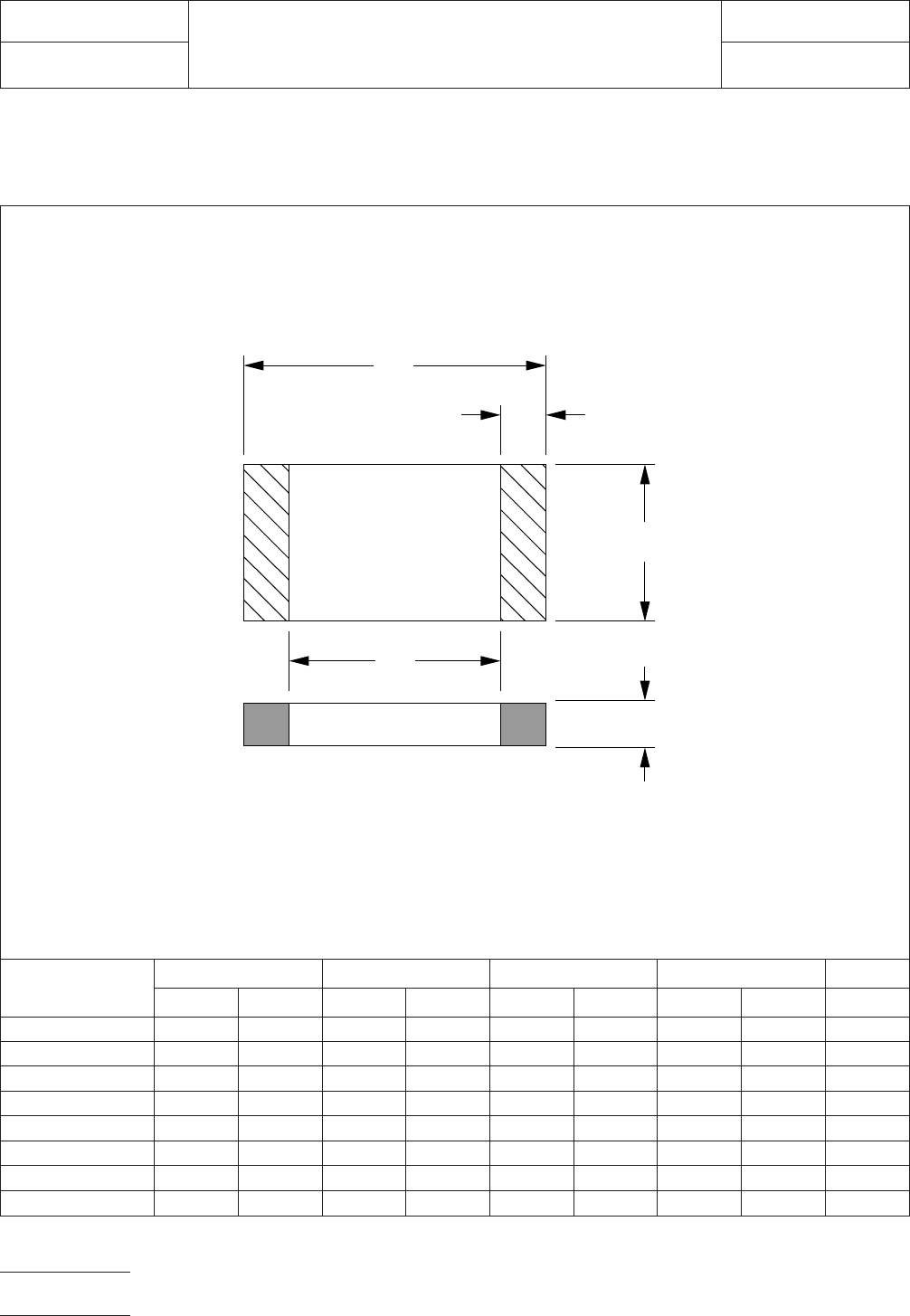
4.0 COMPONENT DIMENSIONS
Figure 2 provides the component dimensions for chip capacitors.
Component
Identifier
(mm) [in]
LSWTH
min max min max min max min max max
1005 [0402] 0.90 1.10 0.30 0.65 0.40 0.60 0.10 0.30 0.60
1310 [0504] 1.02 1.32 0.26 0.72 0.77 1.27 0.13 0.38 1.02
1608 [0603] 1.45 1.75 0.45 0.97 0.65 0.95 0.20 0.50 0.85
2012 [0805] 1.80 2.20 0.30 1.11 1.05 1.45 0.25 0.75 1.10
3216 [1206] 3.00 3.40 1.50 2.31 1.40 1.80 0.25 0.75 1.35
3225 [1210] 3.00 3.40 1.50 2.31 2.30 2.70 0.25 0.75 1.35
4532 [1812] 4.20 4.80 2.30 3.46 3.00 3.40 0.25 0.95 1.35
4564 [1825] 4.20 4.80 2.30 3.46 6.00 6.80 0.25 0.95 1.10
Figure 2 Chip capacitor component dimensions
L
S
T
W
H
IPC-782-8-2-2
IPC-SM-782
Subject
Chip Capacitors
Date
5/96
Section
8.2
Revision
A
Page2of4
电子技术应用 www.ChinaAET.com