IPC-SM-782A 表面安装设计和焊盘设计标准(带BGA).pdf - 第25页
3.3.4 Dimension Tailoring The concepts indicated in this section are reflected in the individual component/land pattern section of this document, sections 8.0 onward. In each instance, the tolerances used for C, F , or P …
If the user of these land patterns desires a more robust pro-
cess condition for placement and soldering equipment,
individual elements of the analysis may be changed to new
and desired dimensional conditions. This includes compo-
nent, board or placement accuracy spread as well as mini-
mum solder joint expectations.
3.3.3.2 Component Dimensions
Illustrations of compo-
nent dimensions beginning in each component section are
accompanied by table of figures for each of the different
part numbers, as taken from EIA-PDP-100, JEDEC-95 and
other world wide component standards.
EIA-PDP-100 is a catalogue listing of outline drawings
illustrating the dimensions of supplier registered passive
components; JEDEC-95 as the outlining document for
solid state products. At times, the component tolerances or
component gauge requirements do not necessarily reflect
the exact tolerance on a manufacturers data sheet. Usually,
this occurs when industry component specification ranges
are so broad that they defy good surface mount design
principles. When this action is taken, the tolerance is indi-
cated with an asterisk (*).
Component dimensions are provided according to the con-
cepts of maximum and least materials condition (MMC and
LMC). Both conditions are presented in the tables. The
component manufacturer may not always dimension his
component in accordance with the limits shown in the
tables, however, these limits may be used as a gauge for
go/no-go acceptance of the component. The LMC dimen-
sions of the figure are those that have been used in the
equations described in 3.3 for determining the recom-
mended land pattern.
Dimensions that have had their tolerance spread reduced
are so indicated in the tables. Parts that are available with
shape characteristics or tolerance limits that fall outside the
recommended norms require land patterns that must be
altered slightly from those presented.
Users of these specialized parts are encouraged to develop
their own land patterns which then become unique to a
specific component vendor part. A dimensioning system
with specific equations has been provided to facilitate
unique land pattern development or enhance process usage.
3.3.3.3 Land Pattern Dimensions
Land pattern dimen-
sions are provided according to the concepts of maximum
material conditions (MMC). Sometimes a dimension is pre-
sented as a minimum distance. This occurs when defining
a space(s) that exists between lands at MMC. The printed
board manufacturer may not always inspect his board in
accordance with the limit concepts shown in the table.
However, these limits may be used as a gauge for go/no-go
acceptance of the printed board land pattern. The dimen-
sions shown in each table are those that have been used in
the equations described in 3.3 for determining the recom-
mended land patterns.
All land patterns are designed to be transparent to the sol-
dering process to be used in manufacturing. This reduces
the number of land sizes in the component library, and is
less confusing for the designer, but may not be the most
robust for the placement or the soldering process.
3.3.3.4 Land Pattern Registration
Each land pattern has
received a registration number. The RLP (Registered Land
Pattern) number is a three digit number with a set of num-
bers assigned to land patterns for a particular family of
components. The original number assigned to a particular
component, uses that analysis shown for the specific sec-
tion (sections 8 through 16). The analyses assume certain
tolerances for board fabrication, placement machine accu-
racy and minimum desired solder joint. Changes in the
assumptions will result in a revision letter to the number.
Thus the first change to RLP 106 would be identified as
RLP 106A, the second change would be RLP 106B etc.
The letters x,y&zarereserved for user modifications to
the standard land pattern. If a company wishes to change
the approved standard land pattern the user would identify
his customized version as RLP 106X, RLP 106Y or RLP
106Z. It should be recognized that X, Y & Z type RLP’s
reflect unique land patterns and will differ company to
company. The number reservations are shown in Table 3-5.
Not every RLP is assigned in Sections 8 through 16, how-
ever all three digit number from 100 to 999 are reserved as
IPC standard RLP numbers. Users of the system may
enhance their computer libraries by tailoring the IPC RLP’s
(adding X, Y or Z), using numbers 001 to 099 or using four
digit numbers to describe their custom standard land pat-
terns. The letter ‘‘W’’ may be used to signify a special user
pattern signifying that it is for wave soldered attachment
application (i.e. RLP 102 defines as RLP 102W.)
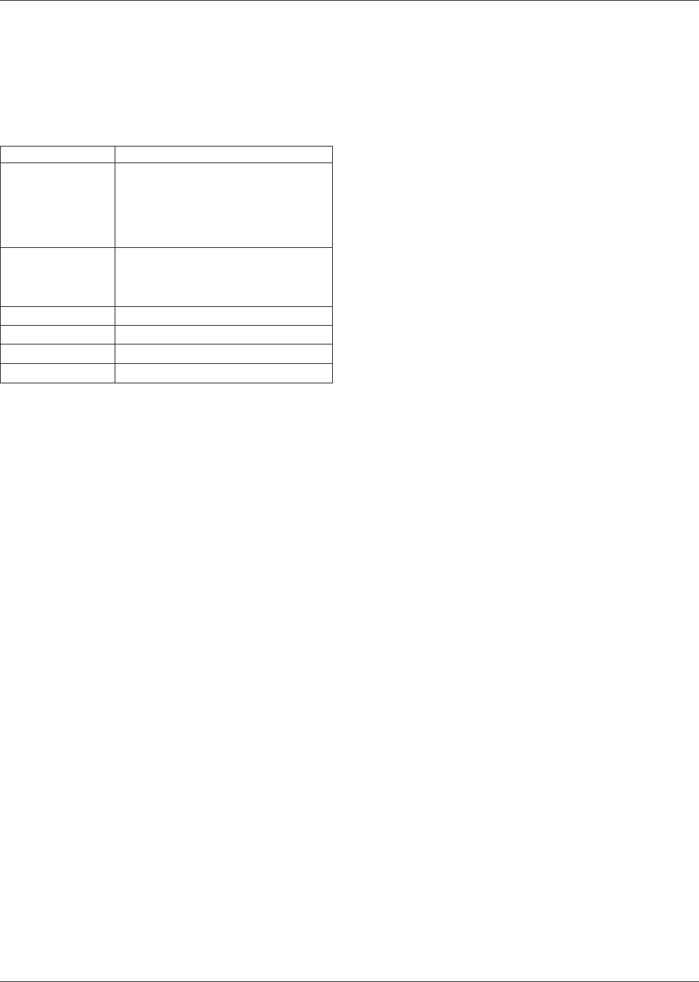
Table 3–4 Tolerance Analysis Elements for Chip Devices
Tolerance Element Detailed Description
Component
Tolerance
The difference between the MMC and
the LMC of each component
dimension, length, width and distance
between electrodes or leads. This
number is the ‘‘C’’ tolerance in the
equations.
Board Tolerance The difference between the MMC and
the LMC of each land pattern
dimension. This number is ‘‘F’’
tolerance in the equations.
Positional Accuracy 0.1 – 0.2 mm DTP
Toe Fillet 0.4 – 0.6 mm
Heel Fillet 0.0 – 0.2 mm
Side Fillet Width –0.02 – 0.02 mm
IPC-SM-782A December 1999
16
电子技术应用 www.ChinaAET.com
3.3.4 Dimension Tailoring
The concepts indicated in
this section are reflected in the individual component/land
pattern section of this document, sections 8.0 onward. In
each instance, the tolerances used for C, F, or P are identi-
fied as well as the desired solder joints—‘‘J.’’ At times the
component tolerances or component gauge requirements do
not necessarily reflect the exact tolerance on a manufactur-
ers data sheet. Usually this occurs when industry compo-
nent specification ranges are so broad that they defy good
surface mount design principles. When the action to
modify the tolerance range is taken, the tolerance ‘‘C’’ is
indicated with an asterisk (*).
In addition, solder joint formation has been considered as
being transparent to the soldering process or equipment
used for mass reflow solder processes. This technique
facilitates a single land pattern for the computer aided
design (CAD) system and allows the assembly to be pro-
cessed by more than one type of assembly operation. As
designs become more complex with denser component/
land pattern geometries, the land patterns may have to be
customized for specific components, and assembly pro-
cesses, in order to make the entire process more robust and
increase first pass defect-free assembly yields.
Users are encouraged to follow the equation principles
defined in this section and in sections 8.0 onward. Main-
taining the data in computer ‘‘spread sheet’’ formats will
facilitate ease of modification to specific land pattern
requirements for process yield improvements.*
Note: Electronic media (3.5 in disk) containing Lotus
spreadsheets are available with instructions for use. They
are identified as IPC-EM-782, ‘‘Land Pattern Data Analy-
sis Spreadsheets for IPC-SM-782 Land Patterns.’’
3.4 Design for Producibility
As part of the planning
cycle of a product’s development, a concurrent engineering
task group should be assembled to determine the criteria
for each new design. During this planning phase, the prod-
uct function and configuration is clearly defined and the
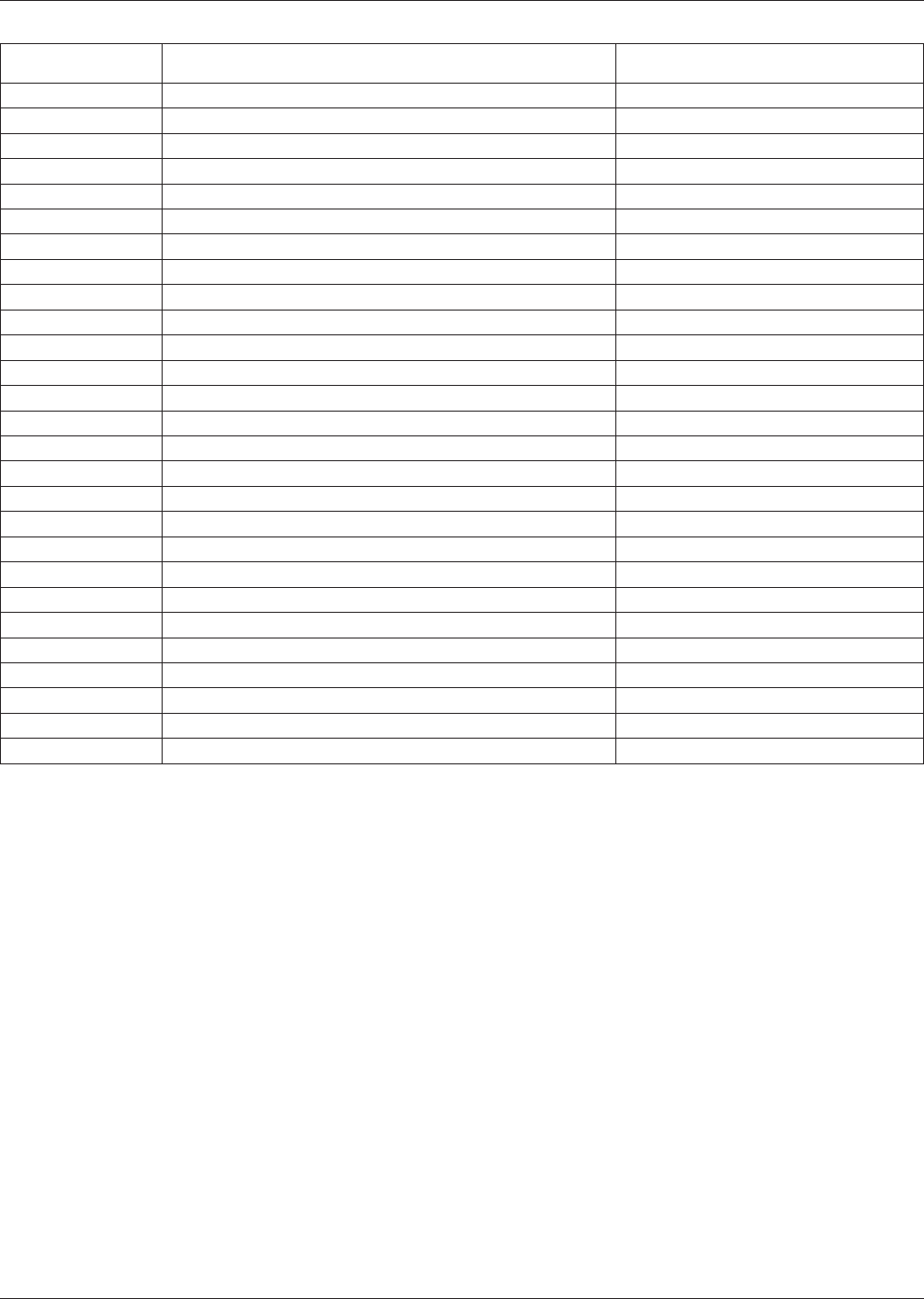
Table 3-5 RLP Numbers
IPC-SM-782 Section Component Type
Reserved Registered
Land Pattern Numbers
8.1 Chip Resisters 100 to 129
8.2 Chip Capacitors 130 to 159
8.3 Inductors 160 to 179
8.4 Tantalum Capacitors 180 to 199
8.5 Metal Electrode Face Components (MELFS) 200 to 209
8.6 Small Outline Transistor (SOT) 23 210 to 214
8.7 Small Outline Transistor (SOT) 89 215 to 219
8.8 Small Outline Diode (SOD) 123 220 to 224
8.9 Small Outline Transistor (SOT) 143 225 to 229
8.10 Small Outline Transistor (SOT) 223 230 to 234
8.11 Modified Through-Hole Component (TO) 252 235 to 239
9.1 Small Outline Integrated Circuits (SOIC) 300 to 329
9.2 Small Outline Integrated Circuits (SSOIC) 330 to 359
9.3 Small Outline Package Integrated Circuit (SOPIC) 360 to 389
9.4 Thin Small Outline Package (TSOP) 390 to 419
9.5 Ceramic Flat Pack (CFP) 420 to 459
10.1 Small Outline with ‘‘J’’ Leads (SOJ) 480 to 529
11.1 Plastic Quad Flat Pack (PQFP) 530 to 549
11.2 Shrink Quad Flat Pack, Square (SQFP) 550 to 579
11.3 Shrink Quad Flat Pack, Rectangular (SQFP) 580 to 629
11.4 Ceramic Quad Flat Pack (CQFP) 630 to 649
12.1 Square Plastic Leaded Chip Carrier (PLCC) 700 to 719
12.2 Rectangular Plastic Leaded Chip Carrier (PLCC) 720 to 739
12.3 Leadless Ceramic Chip Carrier (LCC) 740 to 759
13.1 Modified Dual-In-Line Pin Components (DIP) 760 to 779
14.1 Ball Grid Arrays (BGA) 900 to 1069
14.2 Plastic Rectangular Ball Grid Arrays 1080 to 1082
December 1999 IPC-SM-782A
17
电子技术应用 www.ChinaAET.com

assembly process options outlined. Product size, compo-
nent types, projected volume and the level of manufactur-
ing equipment available may affect process options.
Following the substrate development, the assembly will be
evaluated for many of the fundamentals necessary to insure
a successful SMT process. Specific areas addressed during
the evaluation will include:
• Land pattern concepts
• Component selection
• Mounting substrate design
• Need for testability
• Phototool generation
3.4.1 SMT Land Pattern
The use of process proven land
patterns for the solder attachment of surface mount devices
will provide a benchmark to evaluate solder joint quality.
Land pattern geometry and spacing utilized for each com-
ponent type must accommodate all physical variables
including size, material, lead contact design and plating.
3.4.2 Standard Component Selection
Whenever pos-
sible, SMT devices should be selected from standard con-
figurations. The standard components will be available
from multiple sources and will usually be compatible with
all assembly processes. For those devices developed to
meet specific applications, standard packaging is often
available. Select a package type that will be similar in
materials and plating of standard device types when pos-
sible.
3.4.3 Circuit Substrate Development
Design the circuit
substrate to minimize excessive costs. Surface Mount Tech-
nology often pushes the leading edge of substrate technol-
ogy. When estimating circuit density, allow for the greatest
latitude in fabrication processes and tolerance variables.
Before adopting extreme fine line and utilizing small plated
holes, understand the cost impact, yield, and long-term reli-
ability of the product.
3.4.4 Assembly Considerations
Other factors that will
impact manufacturing efficiency include component place-
ment. Maintaining a consistent spacing between compo-
nents, common orientation or direction of polarized devices
will impact all steps of the assembly process. In addition,
when common orientation is maintained, machine pro-
gramming is simplified and component verification, solder
inspection and repair are simplified.
3.4.5 Provide for Automated Test Testability of the
assembled circuit substrate must be planned well in
advance. If component level testing is necessary, one test
probe contact area is required for each common node or
net. Ideally, all probe contact pads are on one side. Provide
grid-based test nodes to accommodate standard probes.
Functional testing may also employ the same test nodes
used for in-circuit test but will include all connectors that
interface to cables and other assemblies.
3.4.6 Documentation for SMT
Documentation used to
fabricate the circuit substrate and assemble the product
must be accurate and easy to understand. Details, specifi-
cations and notes will guide both the assembly processing
and control the quality level of a product. Unique materials
or special assembly instructions should be included on the
face of the detail drawings or included in the documenta-
tion package.
3.5 Environmental Constraints
3.5.1 Handling Moisture Sensitive Components
Sev-
eral large plastic packages may be susceptible to absorbing
moisture. The component manufacturer usually packages
these parts with a desiccant, and provides instruction for
use or maintaining those parts in a controlled storage envi-
ronment. See J-STD-020 and J-STD-033 for instructions
and proper handling and tesing procedures.
3.5.2 Usage Environments
In Table 3–6, worst-case, but
realistic, use environments for SM electronic assemblies
are shown in nine major use categories. These use environ-
ment categories are listed in order of increasing severity,
without consideration of the number of expected service
years. It should be noted that the cyclic temperature range,
delta T, is not the difference between the possible mini-
mum, Tmin, and maximum, Tmax, operational temperature
extremes; delta T is significantly less. It has to be recog-
nized that these temperature extremes are possible only
during different times of the year, and then only at signifi-
cantly different geographic locations. The delta T values
represent the temperature swings that typically can be
expected during a given operating cycle.
Also given are the expected dwell durations at operating
temperatures; they are significant because they determine
the degree of completeness of the stress relaxation in the
solder joints and thus determine the amount of cyclic
fatigue damage relative to the maximum fatigue damage at
complete stress relaxation. Table 3–6 also gives estimates
of the number of operating cycles occurring during a ser-
vice year. For some of the use categories, the use environ-
ments are described in terms of the sum of multiple use
environments resulting from either significant seasonal
dependence or broadly foreseeable use conditions; the mili-
tary avionics category is subdivided into three subcatego-
ries reflecting differing use conditions due to type of air-
craft, mission profile, geographic effects, etc. The space
category contains two different environments for satellites
in low-earth orbit (LEO) or geo-synchronous (stationary
relative to earth) orbit (GEO).
IPC-SM-782A December 1999
18
电子技术应用 www.ChinaAET.com