IPC-SM-782A 表面安装设计和焊盘设计标准(带BGA).pdf - 第171页
1.0 INTRODUCTION This section covers land patterns for components with J leads on four sides. Each subsection contains information in accor- dance with the following format: 1.0 Scope 2.0 Applicable Documents 3.0 General…
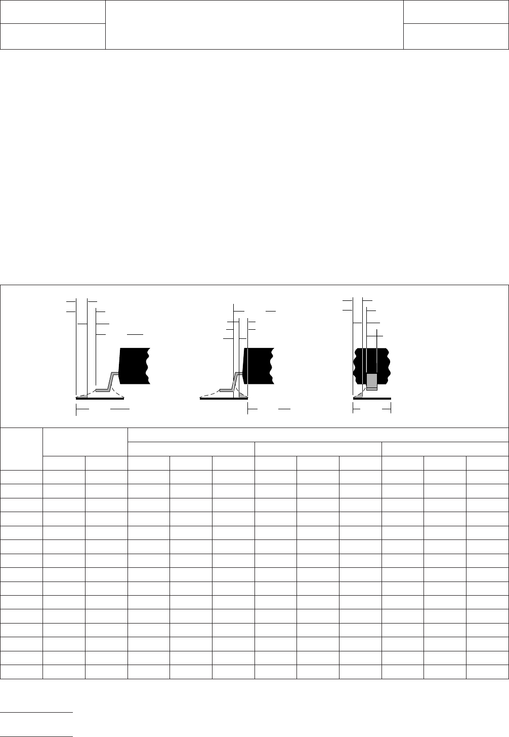
6.0 TOLERANCE AND SOLDER JOINT ANALYSIS
Figure 4 provides an analysis of tolerance assumptions and
resultant solder joints based on the land pattern dimensions
shown in Figure 3. Tolerances for the component dimensions,
the land pattern dimensions (fabrication tolerances on the
interconnecting substrate), and the component placement
equipment accuracy are all taken into consideration.
Figure 4 provides the solder joint minimums for toe, heel, and
side fillets, as discussed in Section 3.3. The tolerances are
addressed in a statistical mode, and assume even distribution
of the tolerances for component, fabrication, and placement
accuracy.
Individual tolerances for fabrication (‘‘F’’) and component
placement equipment accuracy (‘‘P’’) are assumed to be as
given in the table. These numbers may be modified based on
user equipment capability or fabrication criteria. Component
tolerance ranges (C
L
,C
S
, and C
W
) are derived by subtracting
minimum from maximum dimensions given in Figure 2. The
user may also modify these numbers, based on experience
with their suppliers. Modification of tolerances may result in
alternate land patterns (patterns with dimensions other than
the IPC registered land pattern dimensions).
The dimensions for minimum solder fillets at the toe, heel, or
side (J
T
,J
H
,J
S
) have been determined based on industry
empirical knowledge and reliability testing. Solder joint
strength is greatly determined by solder volume. An observ-
able solder fillet is necessary for evidence of proper wetting.
Thus, the values in the table usually provide for a positive sol-
der fillet. Nevertheless, the user may increase or decrease the
minimum value based on process capability.
RLP No.
Tolerance
Assumptions (mm)
Solder Joint
Toe (mm) Heel (mm) Side (mm)
FPC
L
J
T
min J
T
max C
S
J
H
min J
H
max C
W
J
S
min J
S
max
750A 0.10 0.10 0.40 0.46 0.70 0.53 0.59 0.90 0.16 0.00 0.17
751A 0.10 0.10 0.24 0.54 0.72 0.43 0.36 0.62 0.13 0.07 0.23
752A 0.10 0.10 0.24 0.47 0.65 0.43 0.43 0.69 0.13 0.07 0.23
753A 0.10 0.10 0.24 0.50 0.68 0.43 0.40 0.66 0.13 0.07 0.23
754A 0.10 0.10 0.24 0.46 0.64 0.43 0.44 0.70 0.13 0.07 0.23
755A 0.10 0.10 0.24 0.52 0.70 0.43 0.38 0.64 0.13 0.07 0.23
756A 0.10 0.10 0.24 0.48 0.66 0.43 0.42 0.68 0.13 0.07 0.23
757A 0.10 0.10 0.50 0.47 0.73 0.76 0.37 0.75 0.16 –0.01 0.10
758A 0.10 0.10 0.50 0.47 0.73 0.76 0.37 0.75 0.16 –0.01 0.10
759A 0.10 0.10 0.30 0.49 0.66 0.64 0.43 0.76 0.23 –0.01 0.13
760A 0.10 0.10 0.50 0.47 0.73 0.76 0.37 0.75 0.16 –0.01 0.10
761A 0.10 0.10 0.50 0.59 0.85 0.61 0.47 0.79 0.13 0.02 0.12
762A 0.10 0.10 0.50 0.47 0.73 0.76 0.37 0.75 0.16 –0.01 0.10
763A 0.10 0.10 0.50 0.59 0.85 0.61 0.47 0.79 0.13 0.02 0.12
764A 0.10 0.10 0.50 0.47 0.73 0.61 0.60 0.91 0.13 0.02 0.12
Figure 4 Tolerance and solder joint analysis
Zmax
Lmin
▼
▼
▼
▼
1
/2 T
T
J
T
min
Smax
J
H
min
1
/2 T
H
Xmax
▼
▼
Toe Fillet
▼
▼
▼
Heel Fillet
Side Fillet
▼
▼
▼
▼
▼
J
T
max
J
H
max
J
S
min
▼
▼
▼
▼
▼
▼
▼
▼
▼
▼
▼
▼
▼
▼
▼
Gmin
▼
1
/2 T
S
J
S
max
▼
▼
▼
Wmin
▼
IPC-782-11-4-4
IPC-SM-782
Subject
CQFP
Date
5/96
Section
11.4
Revision
A
Page4of4
电子技术应用 www.ChinaAET.com
1.0 INTRODUCTION
This section covers land patterns for components with J leads
on four sides. Each subsection contains information in accor-
dance with the following format:
1.0 Scope
2.0 Applicable Documents
3.0 General Component Description (Figure 1)
4.0 Component Dimensions (Figure 2)
5.0 Land Pattern Dimensions (Figure 3)
6.0 Tolerance and Solder Joint Analysis (Figure 4)
The following is the table of contents for this section:
2.0 APPLICABLE DOCUMENTS
The following documents, of the issue in effect on the revision
date of this section, form a part of this specification to the
extent specified herein.
2.1 Electronic Industries Association (EIA)
1
EIA-481-A
Taping of Surface Mount Components for Auto-
matic Placement
EIA-481-3
32 mm, 44 mm, and 56 mm Embossed Carrier
Taping of Surface Mount Components for Automated Han-
dling
JEDEC Publication 95
Registered and Standard Outlines for
Solid State and Related Products
2.2 International Electrotechnical Commission (IEC)
2
IEC 97
Grid Elements
3.0 General Information
3.1 General Component Description
Leaded Chip Carri-
ers are either ceramic or plastic packages with terminations
which extend beyond the package outlines. These termina-
tions typically space the body of the package from the pack-
aging and interconnect structure for reasons of cleaning,
inspecting, or accommodating differences in thermal expan-
sion. The leads may be attached to the package body either
before or after chip attachment.
In plastic leaded chip carriers, the primary packaging distinc-
tion concerns the point in which a chip is incorporated into the
package. A pre-molded package is supplied as a leaded body
with an open cavity for chip attachment. A post-molded body
part typically has the chip attached to a lead frame with an
insulating plastic body molded around the assembly. It is sup-
plied from the manufacturer without apertures.
Leaded ceramic chip carriers may be similarly classified, but
with a difference in category. The distinction concerns the
point at which leads, if desired, are attached to the ceramic
body. A pre-leaded ceramic chip carrier is supplied with cop-
per or Kovar leads brazed to metallization integral with the
ceramic package. Typically, the package is supplied with an
open cavity for chip attach. A metal or ceramic lid is epoxied,
soldered, or attached with glass frit to provide a hermetic seal
around the chip. After these steps, the leaded assembly is
attached to the printed board.
A post-leaded ceramic chip carrier typically has leads sol-
dered to metallization on the ceramic package after chip
attachment. These leads may take the form of edge clips or
solder columns. Incorporation of leads into the assembly typi-
cally occurs immediately prior to board attachment.
High lead-end coplanarity in surface-mounted lead chip carri-
ers is an important factor in reliable solder attachment to the
printed board. Planarity may be measured from the lowest
three leads of a leaded package. Coplanarity of 0.1 mm
[0.004 in] maximum is recommended with 0.05 mm [0.002 in]
preferred.
1. Application for copies should be addressed to Global Engi-
neering Documents, 1990 M St. N.W., Washington, DC
20036.
2. Application for copes should be addressed to IEC, 3 rue
de Varembe, PO Box 131 - 1211 Geneva 20, Switzerland
IPC-SM-782
Surface Mount Design
and Land Pattern Standard
Date
8/93
Section
12.0
Revision Subject
Components with J Leads
on Four Sides
Page1of2
电子技术应用 www.ChinaAET.com

Page Intentionally Left Blank
IPC-SM-782
Subject
Components with J Leads on Four Sides
Date
8/93
Section
12.0
Revision
Page2of2
电子技术应用 www.ChinaAET.com