IPC-SM-782A 表面安装设计和焊盘设计标准(带BGA).pdf - 第12页
• Small in size, real estate constrained • Able to accommodate large amounts of memory • Light in weight • Able to accommodate several large, high lead count com- plex ICs, such as ASICs and silicon arrays • Able to func…
IPC-782-1-1
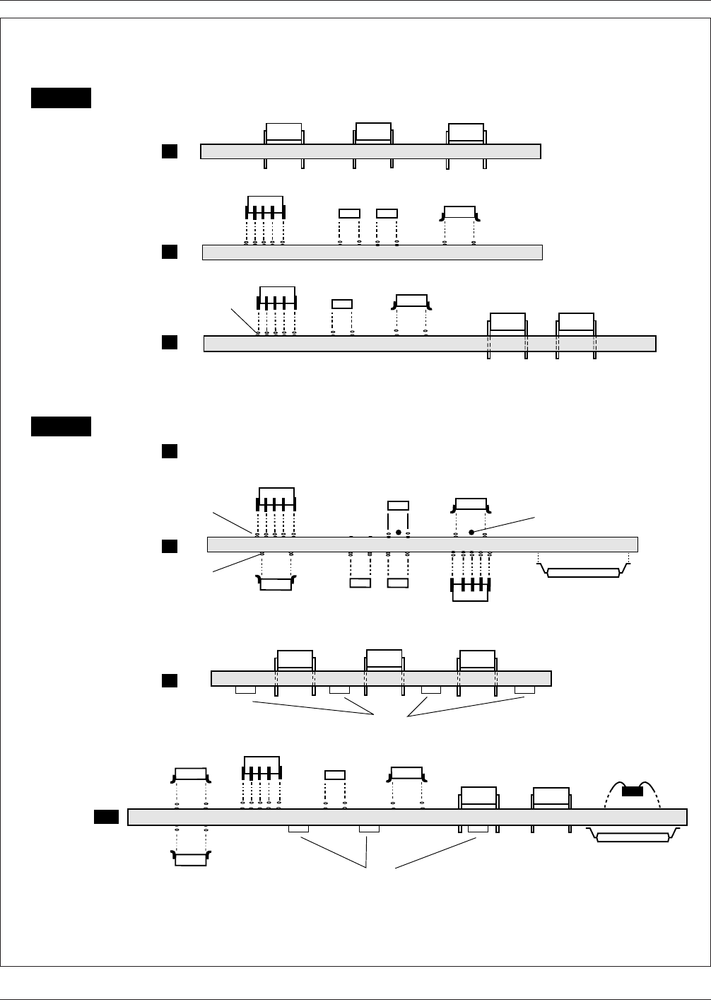
Figure 1–1 Electrical assembly types
PLCC
CHIP COMPONENT
SOIC
DIP
PLCC
CHIP
COMPONENT
SOIC
DIP
PLCC
CHIP COMPONENT
SOIC
PLCC
2-Sided Thru-hole (NOT RECOMMENDED)
SO
CHIP
COMPONENT
PLCC
CHIP
COMPONENT
CHIP
COMPONENT
SOIC
CHIP
COMPONENT
SOIC
DIP
SOLDER
PASTE
SOLDER
PASTE
SOIC
A
B
C
Through-hole
Simple
SMT
Simple
SMT/TH
Complex
Type 1
Type 2
B
C
CX
SMT
Complex
TH/SMT
Simple
SMT/TH
FPT/CMT
Complex
A
SOLDER
PASTE
Adhesive (Optional)
FPT
Simple
Wire bond or
tab IC chip
attachment
FPT PKG.
(selectively attached)
December 1999 IPC-SM-782A
3
电子技术应用 www.ChinaAET.com

• Small in size, real estate constrained
• Able to accommodate large amounts of memory
• Light in weight
• Able to accommodate several large, high lead count com-
plex ICs, such as ASICs and silicon arrays
• Able to function at high frequencies and speeds
• Able to transmit little or no noise, EMI and RFI resistant
• Able to be built in large volumes using automation
Currently, most SMT boards that have 50 or more compo-
nents use a combination of SMT and through-hole tech-
nologies. The mix is a function of component availability,
multiplicity of vendors, and cost. A mix of 80 percent SMT
and 20 percent through-hole parts is very common. How-
ever, the number of 100% SMT assemblies is increasing.
Fine Pitch Technology (FPT) involves a process change as
well as a packaging family, because the package to board
assembly steps are different than SMT. For example, sev-
eral commercially available FPT parts require lead excise
and forming prior to placement. They are encapsulated or
molded with plastic and delivered to users as a separate
packaged device, and these parts may be shipped with a
molded guard-ring or a slide carrier securing the leads in
place. The full encapsulated device will be used for direct
board mounting.
FPT packages are available under package names such as
PQFP (Plastic Quad Flat Pack), CQFP (Ceramic Quad Flat
Pack), QFP (Quad Flat Pack) and VSOIC (Very Small Out-
line Integrated Circuits).
2.0 APPLICABLE DOCUMENTS
The following documents, of the issue currently in effect
form a part of this document to the extend specified herein.
Other documents listed are for reference purposes to assist
the user.
2.1 IPC
1
IPC-A-48 Surface Mount Land Pattern Artwork (Mantech)
IPC-A-49
Surface Mount Land Pattern Artwork (IPC-SM-
782A)
IPC-T-50 Terms and Definitions
IPC-SC-60
Post Solder Solvent Cleaning Handbook
IPC-AC-62
Post Solder Aqueous Cleaning Handbook
IPC-2221
Generic Standard on Printed Board Design
IPC-6012
Qualification and Performance Standard for
Rigid Printed Boards
IPC-D-330
Printed Wiring Design Guide
IPC-A-610
Acceptability of Printed Board Assemblies
IPC-7711
Rework of Electronic Assemblies
IPC-SM-780
Guidelines for Component Packaging and
Interconnection with Emphasis on Surface Mounting
IPC-SM-784
Guidelines for Chip-on-Board Technology
Implementation
IPC-SM-785
Guidelines for Accelerated Reliability Testing
of Surface Mount Solder Attachments
IPC-SM-786
Recommended Procedures for Handling of
Moisture Sensitive Plastic IC Packages
IPC-AJ-820
Assembly and Joining Handbook
IPC-CC-830
Electrical Insulating Compounds for Printed
Board Assemblies
IPC-SM-840
Qualification and Performance of Permanent
Polymer Coating (Solder Mask) for Printed Boards
IPC-1902/IEC 60097
Grid System for Printed Circuits
2.2 Electronic Industries Association
2
IS-30
Surface Mount Resistors
JEDEC-95
JEDEC Registered and Standard Outlines for
Solid State Products
EIA-PDP-100
Registered and Standard Mechanical Out-
lines for Electronic Parts
RS-198
Ceramic Dielectric Capacitors
RS-228
Fixed Electrolytic Tantalum Capacitors
RS-367
Dimensional and Electrical Characteristics Defin-
ing Receiver Type Sockets
RS-376
Fixed Film Dielectric Capacitors in Metallic and
Non- Metallic Cases for D.C. Application
RS-415
Dimensional and Electrical Characteristic Defin-
ing Dual-In-Line-Type Sockets
RS-428
Type Designation System for Microelectronic
Devices
1. IPC, 2215 Sanders Road, Northbrook, IL 60062-6135
2. Electronic Industries Association, 2001 Eye Street N.W., Washington, DC 20006
IPC-SM-782A December 1999
4
电子技术应用 www.ChinaAET.com

RS-471
Symbol and Label for Electrostatic Sensitive
Devices
RS-481
Tape and Reel Specification
2.3 Joint Industry Standards (IPC)
1
J-STD-001
Requirements for Soldered Electrical and Elec-
tronic Assemblies
J-STD-002
Solderability Tests for Component Leads, Ter-
minations, Lugs, Terminals and Wires
J-STD-003 Solderability Tests for Printed Boards
2.4 American Society of Mechanical Engineers
3
ANSI Y14.5M—1982 Dimensioning and Tolerancing
3.0 DESIGN REQUIREMENTS
3.1 Terms and Definitions
Terms and definitions used
herein are in accordance with IPC-T-50 except as otherwise
specified. Note: Any definition denoted with an asterisk (*)
is a reprint of the definition defined in IPC-T-50.
*Assembly – A number of parts of subassemblies or any
combination thereof joined together.
Note: When this term is used in conjunction with other
terms listed herein, the following definitions shall prevail.
Assembly, double-sided – A packaging and interconnecting
structure with components mounted on both the primary
and secondary sides.
Assembly, multilayer printed circuit – a multilayer printed
circuit board on which separately manufactured compo-
nents and parts have been added.
Assembly, multilayer printed wiring – a multilayer printed
wiring board on which separately manufactured compo-
nents and parts have been added.
Assembly, packaging and interconnecting (P&IA) – The
generic term for an assembly that has electronic compo-
nents mounted on either one or both sides of a packaging
and interconnecting structure.
Assembly, printed board – an assembly of several printed
circuit assemblies or printed wiring assemblies, or both.
Assembly, printed circuit – a printed circuit board on
which
separately manufactured components and parts have been
added.
Assembly, printed wiring – a printed wiring board on
which
separately manufactured components and parts have been
added.
Assembly, single-sided – A packaging and interconnecting
structure with components mounted only on the primary
side.
*Base material – The insulating material upon which the
conductor pattern may be formed. The base material may
be rigid or flexible. It may be a dielectric sheet or insulated
metal sheet.
Basic dimension – Theoretically exact location of a com-
ponent feature, indicated by a symbol or a number in a box.
(The tolerance on a basic dimension provides the limits of
the variation from the basic dimension location.)
Castellation – Metallized features that are recessed on the
edges of a chip carrier which are used to interconnect con-
ducting surfaces or planes within or on the chip carrier.
Chip carrier – A low-profile rectangular component pack-
age, usually square, whose semiconductor chip cavity or
mounting area is a large fraction of the package size and
whose external connections are usually on all four sides of
the package.
Chip-on-board (COB) – Integrated circuit device mounted
directly to the printed board and interconnected with wire
bonds.
Coefficient of thermal expansion (CTE) – The linear ther-
mal expansion per unit change in temperature.
Component – A separable part of a printed board assembly
which performs a circuit function (e.g., a resistor, capaci-
tor, transistor, etc.)
Component mounting site – A location on a P&I structure
that consists of a land pattern and conductor fan-out to
additional lands for testing or vias that are associated with
the mounting of a single component.
*Conductive pattern – The configuration or design of the
conductive material on the base material. (Includes conduc-
tors, lands, and through connections when these connec-
tions are in integral part of the manufacturing process.)
*Conductor – A single conductive path in a conductive
pattern.
Constraining core – A supporting plane that is internal to
a packaging and interconnecting structure.
*Dual in-line package (DIP) – A component which termi-
nates in two straight and parallel rows of pins or lead
wires.
Fine-pitch technology (FPT) – Surface mounted compo-
nents with a lead or termination pitchof 0.63 mm or less.
Fiducial – A feature of the PB used to provide common
measurable points for all steps in the assembly process.
Flat pack – A component with two straight rows of leads
(normally on 1.27 mm centers) which are parallel to the
component body.
3. Publications are available from the American Society of Mechanical Engineers, 345 East 47th St., New York, NY 10017
December 1999 IPC-SM-782A
5
电子技术应用 www.ChinaAET.com