IPC-SM-782A 表面安装设计和焊盘设计标准(带BGA).pdf - 第58页
The acceptable number of cycles can be increased by reducing the thermal expansion mismatch, reducing the temperature gradient, increasing the solder joint height, using the smallest physical size part where possible, an…
6.1 General Considerations
P&I Structures vary from
basic printed wiring boards to very sophisticated
supporting-core structures. However, some selection crite-
ria are common to all structures. To aid in the selection
process, Table 6–2 lists design parameters and material
properties which affect system performance, regardless of
P&IS type. Also, Table 6–3 lists the properties of the mate-
rials most-common for these applications.
6.1.1 Categories
In general, a P&I structure will fit into
one of four basic categories of construction: organic base
material, non-organic base material, supporting plane, and
constraining core.
6.1.2 Thermal Expansion Mismatch
A primary concern
of surface mounted leadless parts is the thermal expansion
mismatch between the leadless part and the P&I structure.
This mismatch will fracture solder joint interconnections if
the assembly is subjected to thermal shock, thermal
cycling, power cycling and high operating temperatures.
The number of fatigue cycles before solder joint failure
depends on the thermal expansion mismatch between the
part and the P&I structure, the temperature range over
which the assembly must operate, the solder joint thick-
ness, the size of the part and the power cycling. For
example, power cycling may cause an undesirable thermal
expansion mismatch if a significant temperature difference
exists between a chip carrier and the P&I structure.
IPC-782-5-2
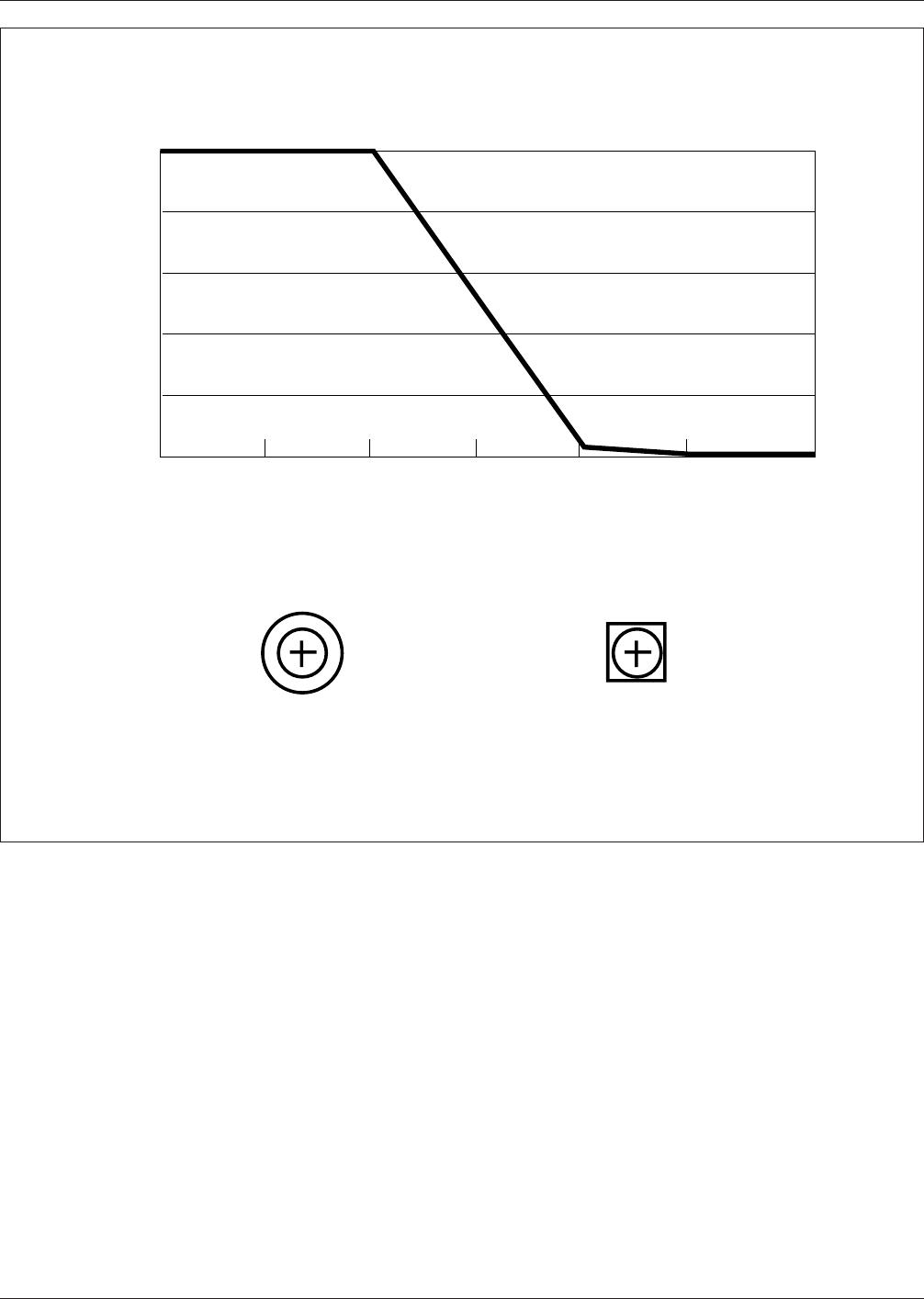
Figure 5–2 General relationship between test contact size and test probe misses
Probability of at Least One Miss
Test/Via Probe Contact Size
100%
80%
60%
40%
20%
0%
0.25mm 0.35mm 0.5mm 0.6mm
Diameter
0.75mm 0.9mm 1.0mm
1.0mm Dia
[0.04"]
0.9mm Square
[.036"]
**
*
*
*
December 1999 IPC-SM-782A
49
电子技术应用 www.ChinaAET.com
The acceptable number of cycles can be increased by
reducing the thermal expansion mismatch, reducing the
temperature gradient, increasing the solder joint height,
using the smallest physical size part where possible, and by
optimizing the thermal path between the part and P&I
structure. The overall systems operating requirements for
each class of hardware determines the acceptable number
of cycles.
6.2 Organic-Base Material P&IS
Organic-base materials
work best with leaded chip carriers. With leadless chip car-
riers, however, the thermal expansion mismatch between
package and substrate can cause problems. Also, flatness,
rigidity, and thermal conductivity requirements may limit
their use. Finally, you must pay attention to package size,
I/O count, thermal cycling stability, maximum operating
temperature and solder joint compliance.
6.3 Non-Organic Base Materials
Non-organic base
materials typically used with thick-or thin-film technology
are also ideally suited for leaded and leadless chip carrier
designs. They can incorporate thick- or thin-film resistors
directly on the P&I structure and buried capacitor layers
that increase density and improve reliability. However,
repairability of the P&I structure is limited. Ceramic mate-
rials, usually alumina, appear ideal for P&I structure with
leadless ceramic chip carriers because of their relatively-
high thermal conductivity (see Table 6–3) and the coeffi-
cient of thermal expansion (CTE) match. Unfortunately, the
P&I structure is limited to approximately 22,600 sq. mm.
[35 square inches]. However, the evolving use of these
materials with non-noble metals, such as copper, has
attracted both military and commercial applications.
Ceramic P&I structures currently have three applications:
ceramic hybrid circuits, ceramic multichip modules
(MCM-L) and ceramic printed boards.
6.4 Supporting-Plane P&I Structures
Supporting metal-
lic or non-metallic planes can be used with conventional
printed boards or with custom processing to enhance P&IS
properties. Depending on the results desired, the supporting
plane can be electrically-functional or not and can also
serve as a structure stiffener, heatsink and/or CTE con-
straint.
High-density, sequentially-processed, multilayer P&I struc-
tures are available with organic dielectrics of specific thick-
ness, ultrafine conductors, and solid plated vias for layer-
to-layer interconnections with thermal lands for heat trans-
fer, all connected to a low-CTE metal support heatsink.
Thus, this technology combines laminating materials,
chemical processing, photolithography, metallurgy, and
unique thermal transfer innovations, such that it is also
appropriate for mounting and interconnecting bare inte-
grated circuit chips.
The major advantage of this system is that the vias can be
as small as 0.20 mm [0.005 inches] square and conductor
widths can range from 0.12 to 0.20 mm [0.003 to 0.005
inches] for high interconnection density. Thus, most appli-
cations can be satisfied with two signal layers with addi-
tional layers for power and ground.
Discrete-wire P&I structures have been developed specifi-
cally for use with surface mounted components, as shown
in Figure 5–3. These structures are usually built with a
low-expansion metal support plane that also offers good
heat dissipation.
The interconnections are made by discrete 0.06 mm
[0.0025 inch] diameter insulated copper wires precisely
placed on a 0.03 mm [inch] grid by numerically-controlled
IPC-782-5-3
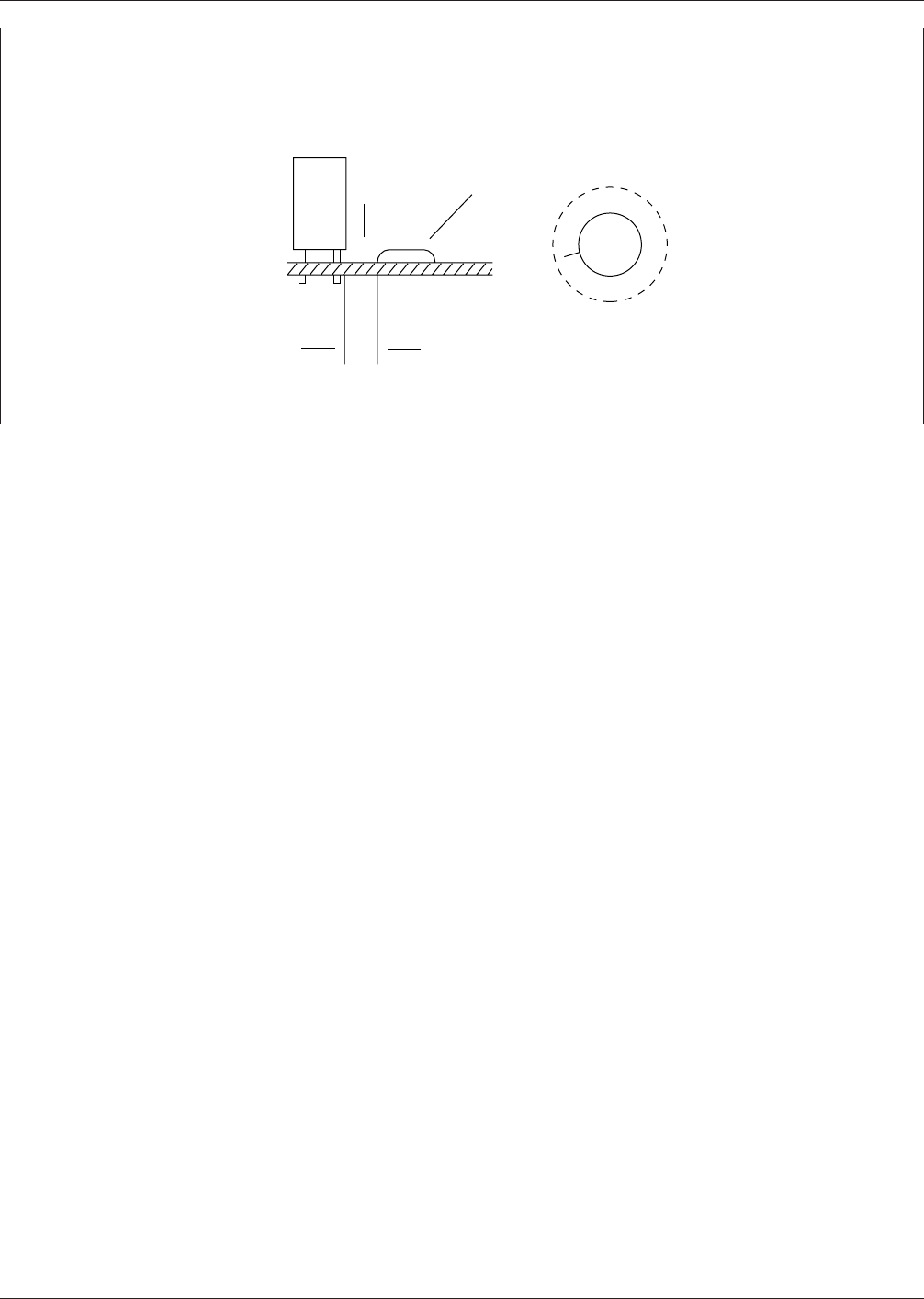
Figure 5–3 Test probe feature distance from component
Component
Height
▼
▼
▼
Free
Area
6.5mm [0.255"] height
> 5.0mm
[0.20"] Min.
Test
Pad
5.0mm [0.20"]
Tall Component
Free area
▼
Diagram Showing Free Area around Test Pad
for Components Greater than 6.5mm in Height
▼
Test Pad
IPC-SM-782A December 1999
50
电子技术应用 www.ChinaAET.com
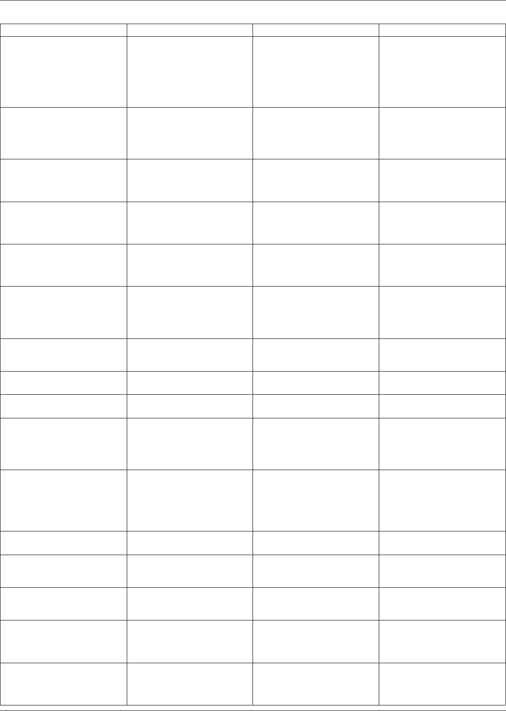
Table 6–1 Packaging and Interconnecting Structure Comparison
Type Major Advantages Major Disadvantages Comments
Organic Base Substrate
Epoxy Fiberglass Substrate size, weight,
reworkable, dielectric
properties, conventional board
processing
Thermal conductivity, X, Y and
Z axis CTE
Because of its high X–Y plane
CTE, it should be limited to
environments and applications
with small changes in
temperature and/or small
packages.
Polyimide Fiberglass Same as Epoxy Fiberglass plus
high temperature X–Y axis
CTE, substrate size, weight,
reworkable, dielectric
properties, high Tg.
Thermal conductivity, Z-axis
CTE, moisture absorption
Same as Epoxy Fiberglass
Epoxy Aramid Fiber Same as Epoxy Fiberglass,
X–Y axis CTE, substrate size,
lightest weight, reworkable,
dielectric properties
Thermal conductivity, Z-axis
CTE, resin microcracking, Z
axis CTE, water absorption
Volume fraction of fiber can be
controlled to tailor X–Y CTE.
Resin selection critical to
reducing resin micro-cracks
Polyimide Aramid Fiber Same as Epoxy Aramid Fiber,
X–axis CTE, substrate size,
weight, reworkable, dielectric
properties
Thermal conductivity, Z–axis
CTE, resin microcracking,
water absorption
Same as Epoxy Aramid Fiber
Polyimide Quartz (Fused Silica) Same as Polyimide Aramid
Fiber, X–Y axis CTE, substrate
size, weight, reworkable,
dielectric properties
Thermal conductivity, Z axis
CTE, drilling, availability, cost,
low resin content required
Volume fraction of fiber can be
controlled to tailor X–Y CTE.
Drill wearout higher than with
fiberglass.
Fiberglass/Aramid Composite
Fiber
Same as Polyimide Aramid
Fiber, no surface microcracks,
Z axis CTE, substrate size,
weight, reworkable, dielectric
properties
Thermal conductivity, X and Y
axis CTE, water absorption,
process solution entrapment
Resin microcracks are confined
to internal layers and cannot
damage external circuitry.
Fiberglass/Teflon® Laminates Dielectric constant, high
temperature
Same as Epoxy Fiberglass, low
temperature stability, thermal
conductivity, X and Y axis CTE
Suitable for high speed logic
applications.
Same as Epoxy Fiberglass.
Flexible Dielectric Light weight, minimal concern
to CTE, configuration flexibility
Size, cost, Z-axis expansion Rigid-flexible boards offer
trade-off compromises.
Thermoplastic 3–D configurations, low
high-volume cost
High injection-molding setup
costs
Relatively new for these
applications
Non-Organic Base
Alumina (Ceramic) CTE, thermal conductivity,
conventional thick film or thin
film processing, integrated
resistors
Substrate size, rework
limitations, weight, cost, brittle,
dielectric constant
Most widely used for hybrid
circuit technology
Supporting Plane
Printed Board Bonded to Plane
Support (Metal or Non-Metal)
Substrate size, reworkability,
dielectric properties,
conventional board processing,
X–Y axis CTE, stiffness,
shielding, cooling
Weight The thickness/CTE of the metal
core can be varied along with
the board thickness, to tailor
the overall CTE of the
composite.
Sequential Processed Board
with Supporting Plane Core
Same as board bonded to
supporting plane
Weight Same as board bonded to
supporting plane.
Discrete Wire High-speed interconnections.
Good thermal and electrical
features.
Licensed process.
Requires special equipment.
Same as board bonded to
low-expansion metal support
plane.
Constraining Core
Porcelainized Copper Clad
Invar
Same as Alumina. Reworkability, compatible thick
film materials.
Thick film materials are still
under development.
Printed Board Bonded with
Constraining Metal Core
Same as board bonded to low
expansion metal cores,
stiffness, thermal conductivity,
low weight.
Cost, microcracking. The thickness of the graphite
and board can be varied to
tailor the overall CTE of the
composite.
Compliant Layer Structures Substrate size, dielectric
properties, X–Y axis, CTE.
Z axis CTE, thermal
conductivity.
Compliant layer absorbs
difference in CTE between
ceramic package and
substrate.
December 1999 IPC-SM-782A
51
电子技术应用 www.ChinaAET.com