IPC-SM-782A 表面安装设计和焊盘设计标准(带BGA).pdf - 第118页
4.0 COMPONENT DIMENSIONS Figure 2 provides the component dimensions for SOIC components. Component Identifier JEDEC Number L (mm) S (mm) W (mm) T (mm) A (mm) B (mm) H (mm) P (mm) min max min max min max min max min max mi…
1.0 SCOPE
This subsection provides the component and land pattern
dimensions for small outline integrated circuits (SOIC compo-
nents) with gullwing leads. Basic construction of the SOIC
device is also covered. At the end of this subsection is a list-
ing of the tolerances and target solder joint dimensions used
to arrive at the land pattern dimensions.
2.0 APPLICABLE DOCUMENTS
See Section 9.0 for documents applicable to the subsections.
3.0 COMPONENT DESCRIPTIONS
These components are all on 1.27 mm pitch, and are available
in narrow body (3.90 mm), wide body (7.50 mm) and extra
wide body (8.90 mm) sizes, ranging from 8 to 36 pins.
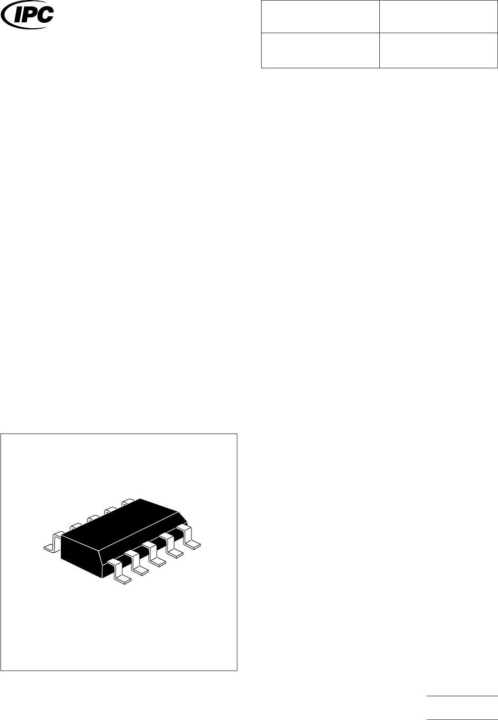
3.1 Basic Construction
See Figure 1. Basic construction
consists of a plastic body and metallic leads.
3.1.1 Termination Materials
Leads should be solder-
coated with a tin/lead alloy. The solder should contain
between 58 to 68% tin. Solder may be applied to the termi-
nation by hot dipping or by plating from solution. Plated sol-
der terminations should be subjected to a post-plating reflow
operation to fuse the solder. The tin/lead finish should be at
least 0.00075 mm [0.0003 in] thick.
Solder finish applied over precious-metal leads shall have a
diffusion-barrier layer between the lead metallization and the
solder finish. The barrier layer should be nickel or an equiva-
lent diffusion barrier, and should be at least 0.00125 mm
[0.00005 in] thick.
3.1.2 Marking
All parts shall be marked with a part number
and ‘‘Pin 1’’ location. ‘‘Pin 1’’ location may be molded into the
plastic body.
3.1.3 Carrier Package Format
Bulk rods, 24 mm tape/
8–12 mm pitch is preferred for best handling. Tube carriers
are also used.
3.1.4 Resistance to Soldering
Parts should be capable of
withstanding ten cycles through a standard reflow system
operating at 215°C. Each cycle shall consist of 60 seconds
exposure at 215°C. Parts must also be capable of withstand-
ing a minimum of 10 seconds immersion in molten solder at
260°C.
IPC-782-9-1-1
Figure 1 SOIC construction
IPC-SM-782
Surface Mount Design
and Land Pattern Standard
Date
5/96
Section
9.1
Revision
A
Subject
SOIC
Page1of4
电子技术应用 www.ChinaAET.com
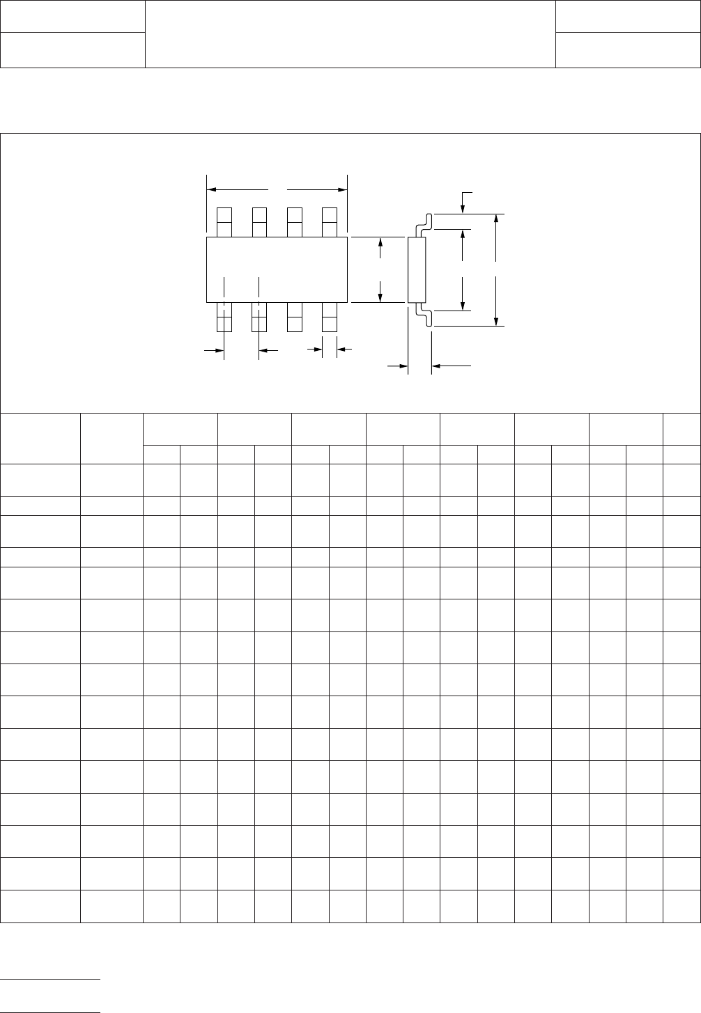
4.0 COMPONENT DIMENSIONS
Figure 2 provides the component dimensions for SOIC components.
Component
Identifier
JEDEC
Number
L (mm) S (mm) W (mm) T (mm) A (mm) B (mm) H (mm)
P
(mm)
min max min max min max min max min max min max min max basic
S08 MS-012
AA
5.80 6.20 3.26 4.55 0.33 0.51 0.40 1.27 3.80 4.00 4.80 5.00 1.35 1.75 1.27
S08W — 10.00 10.65 7.46 8.85 0.33 0.51 0.40 1.27 7.40 7.60 5.05 5.45 2.35 2.65 1.27
S014 MS-012
AB
5.80 6.20 3.26 4.55 0.33 0.51 0.40 1.27 3.80 4.00 8.55 8.75 1.35 1.75 1.27
S014 W — 10.00 10.65 7.46 8.85 0.33 0.51 0.40 1.27 7.40 7.60 8.80 9.20 2.35 2.65
S016 MS-012
AC
5.80 6.20 3.26 4.55 0.33 0.51 0.40 1.27 3.80 4.00 9.80 10.00 1.35 1.75 1.27
S016W MS-013
AA
10.00 10.65 7.46 8.85 0.33 0.51 0.40 1.27 7.40 7.60 10.10 10.50 2.35 2.65 1.27
S020W MS-013
AC
10.00 10.65 7.46 8.85 0.33 0.51 0.40 1.27 7.40 7.60 12.60 13.00 2.35 2.65 1.27
S024W MO-119
AA
10.29 10.64 8.21 9.01 0.36 0.51 0.53 1.04 7.40 7.60 15.54 15.85 2.34 2.64 1.27
S024X MO-120
AA
11.81 12.17 9.73 10.54 0.36 0.51 0.53 1.04 8.76 9.02 15.54 15.85 2.34 2.64 1.27
S028W MO-119
AB
10.29 10.64 8.21 9.01 0.36 0.51 0.53 1.04 7.40 7.60 18.08 18.39 2.34 2.64 1.27
S028X MO-120
AB
11.81 12.17 9.73 10.54 0.36 0.51 0.53 1.04 8.76 9.02 18.08 18.39 2.34 2.64 1.27
S032W MO-119
AC
10.29 10.64 8.21 9.01 0.36 0.51 0.53 1.04 7.40 7.60 20.62 20.93 2.34 2.64 1.27
S032X MO-120
AC
11.81 12.17 9.73 10.54 0.36 0.51 0.53 1.04 8.76 9.02 20.62 20.93 2.34 2.64 1.27
S036W MO-119
AD
10.29 10.64 8.21 9.01 0.36 0.51 0.53 1.04 7.40 7.60 23.16 23.47 2.34 2.64 1.27
S036X MO-120
AD
11.81 12.17 9.73 10.54 0.36 0.51 0.53 1.04 8.76 9.02 23.16 23.47 2.34 2.64 1.27
Figure 2 SOIC component dimensions
P
H
SL
W
B
A
T
IPC-782-9-1-2
IPC-SM-782A
Subject
SOIC
Date
5/96
Section
9.1
Revision
A
Page2of4
电子技术应用 www.ChinaAET.com
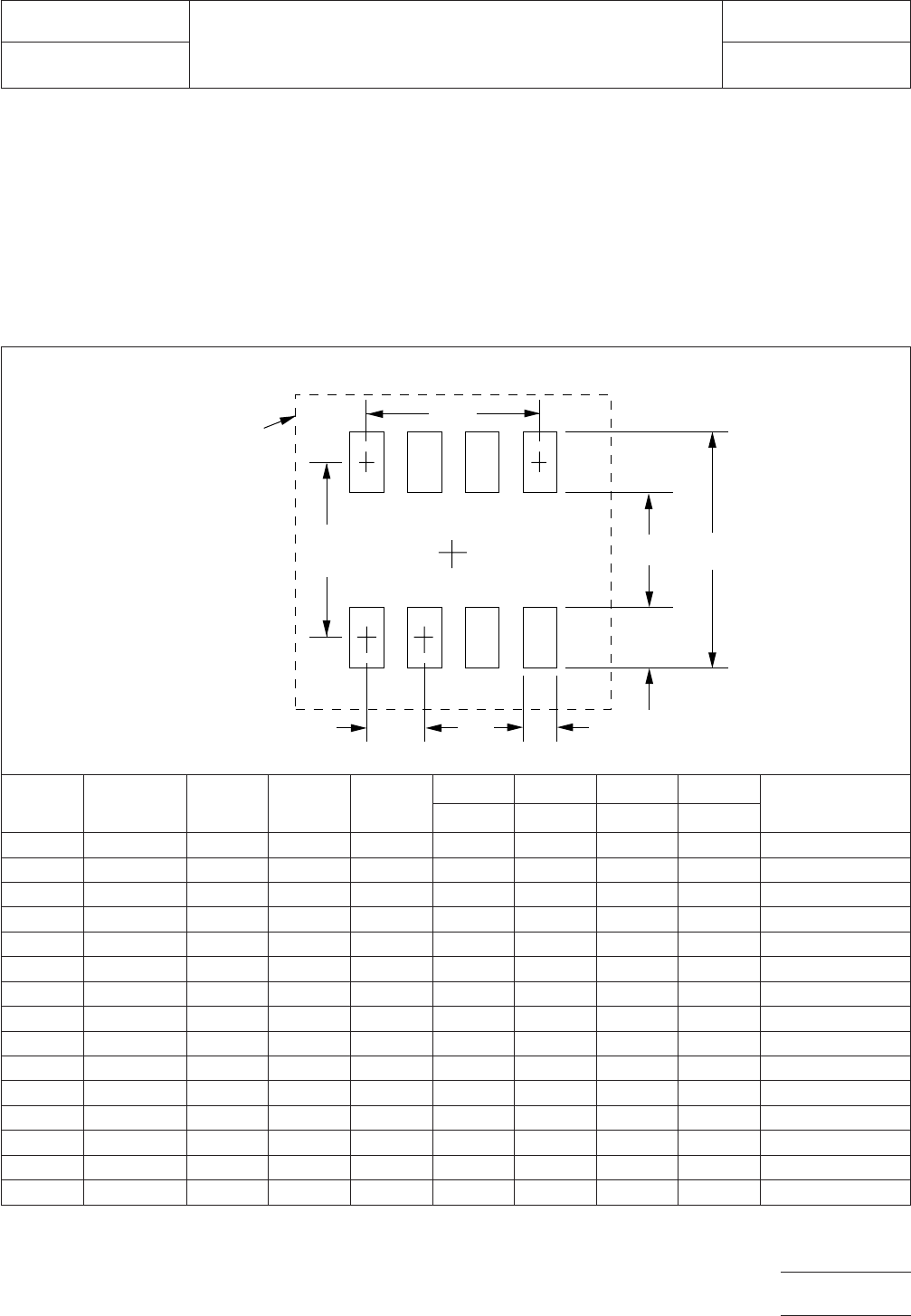
5.0 LAND PATTERN DIMENSIONS
Figure 3 provides the land pattern dimensions for SOIC com-
ponents. These numbers represent industry consensus on the
best dimensions based on empirical knowledge of fabricated
land patterns.
In the table, the dimensions shown are at maximum material
condition (MMC). The least material condition (LMC) should
not exceed the fabrication (F) allowance shown on page 4.
The LMC and the MMC provide the limits for each dimension.
The dotted line in Figure 3 shows the grid placement court-
yard which is the area required to place land patterns and
their respective components in adjacent proximity without
interference or shorting. Numbers in the table represent the
number of grid elements (each element is 0.5 by 0.5 mm) in
accordance with the international grid detailed in IEC publica-
tion 97.
RLP No.
Component
Identifier Z (mm) G (mm) X (mm)
Y (mm) C (mm) D (mm) E (mm)
Placement Grid
(No. Grid
Elements)
ref ref ref ref
300A S08 7.40 3.00 0.60 2.20 5.20 3.81 1.27 16x12
301A S08W 11.40 7.00 0.60 2.20 9.20 3.81 1.27 24x12
302A S014 7.40 3.00 0.60 2.20 5.20 7.62 1.27 16x20
303A S014W 11.40 7.00 0.60 2.20 9.20 7.62 1.27 24x20
304A S016 7.40 3.00 0.60 2.20 5.20 8.89 1.27 16x22
305A S016W 11.40 7.00 0.60 2.20 9.20 8.89 1.27 24x22
306A S020W 11.40 7.00 0.60 2.20 9.20 11.43 1.27 24x28
307A S024W 11.40 7.00 0.60 2.20 9.20 13.97 1.27 24x32
308A S024X 13.00 8.60 0.60 2.20 10.80 13.97 1.27 28x32
309A S028W 11.40 7.00 0.60 2.20 9.20 16.51 1.27 24x38
310A S028X 13.00 8.60 0.60 2.20 10.80 16.51 1.27 28x38
311A S032W 11.40 7.00 0.60 2.20 9.20 19.05 1.27 24x44
312A S032X 13.00 8.60 0.60 2.20 10.80 19.05 1.27 28x44
313A S036W 11.40 7.00 0.60 2.20 9.20 21.59 1.27 24x48
314A S036X 13.00 8.60 0.60 2.20 10.80 21.59 1.27 28x48
Figure 3 SOIC land pattern dimensions
x
GZ
Y
E
D
C
Grid
placement
courtyard
IPC-782-9-1-3
IPC-SM-782A
Subject
SOIC
Date
5/96
Section
9.1
Revision
A
Page3of4
电子技术应用 www.ChinaAET.com